

Active Member
|
[China]

Address: #506B, Henghui Business Center, No.77, Lingxia Nan Road, High Technology Zone, Huli, Xiamen 361006, China
Contact name:

XIAMEN POWERWAY ADVANCED MATERIAL CO., LTD. |
|
|
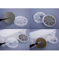
4H High Purity Semi Insulating SiC Wafer, Production Grade,3”Size, Low Carrier Concentration
PAM-XIAMEN provides high quality single crystal SiC (Silicon Carbide)waferfor electronic and optoelectronic industry. SiC wafer is a next generation semiconductor materialwith unique electrical properties and excellent thermal properties for high temperature and high power device application. SiC wafer can be supplied in diameter 2~6 inch, both 4H and 6H SiC , N-type , Nitrogen doped , and semi-insulating type available. Please contact us for more information
High Purity Semi Insulating SiC Wafer: Due to the wide band gap, the intrinsic carrier concentration of SiC wafer is very low at room temperature. This value is about 0.13cm-3 for 3C SiC, about 5x10^-2cm2 for 4H SiC and about 1x10^- 6 cm-3 for 6H SiC. This is the main reason why SiC electronic devices can work at high temperature and the leakage current is very small.
SILICON CARBIDE MATERIAL PROPERTIES
| Polytype | Single Crystal 4H | Single Crystal 6H |
| Lattice Parameters | a=3.076 Å | a=3.073 Å |
| c=10.053 Å | c=15.117 Å | |
| Stacking Sequence | ABCB | ABCACB |
| Band-gap | 3.26 eV | 3.03 eV |
| Density | 3.21 · 103 kg/m3 | 3.21 · 103 kg/m3 |
| Therm. Expansion Coefficient | 4-5×10⁻⁶/K | 4-5×10⁻⁶/K |
| Refraction Index | no = 2.719 | no = 2.707 |
| ne = 2.777 | ne = 2.755 | |
| Dielectric Constant | 9.6 | 9.66 |
| Thermal Conductivity | 490 W/mK | 490 W/mK |
| Break-Down Electrical Field | 2-4 · 108 V/m | 2-4 · 108 V/m |
| Saturation Drift Velocity | 2.0 · 105 m/s | 2.0 · 105 m/s |
| Electron Mobility | 800 cm2/V·S | 400 cm2/V·S |
| hole Mobility | 115 cm2/V·S | 90 cm2/V·S |
| Mohs Hardness | ~9 | ~9 |
4H High Purity Semi Insulating SiC Wafer, Production Grade,3”Size
| SUBSTRATE PROPERTY | S4H-51-SI-PWAM-250 S4H-51-SI-PWAM-330 S4H-51-SI-PWAM-430 |
| Description | Production Grade 4H SEMI Substrate |
| Polytype | 4H |
| Diameter | (50.8 ± 0.38) mm |
| Thickness | (250 ± 25) μm (330 ± 25) μm (430 ± 25) μm |
| Resistivity (RT) | >1E5 Ω·cm |
| Surface Roughness | < 0.5 nm (Si-face CMP Epi-ready); <1 nm (C- face Optical polish) |
| FWHM | <30 arcsec <50 arcsec |
| Micropipe Density | A+≤1cm-2 A≤10cm-2 B≤30cm-2 C≤50cm-2 D≤100cm-2 |
| Surface Orientation | |
| On axis <0001>± 0.5° | |
| Off axis 3.5° toward <11-20>± 0.5° | |
| Primary flat orientation | Parallel {1-100} ± 5° |
| Primary flat length | 16.00 ± 1.70 mm |
| Secondary flat orientation Si-face:90° cw. from orientation flat ± 5° | |
| C-face:90° ccw. from orientation flat ± 5° | |
| Secondary flat length | 8.00 ± 1.70 mm |
| Surface Finish | Single or double face polished |
| Packaging | Single wafer box or multi wafer box |
| Usable area | ≥ 90 % |
| Edge exclusion | 1 mm |
SiC crystal growth
Bulk crystal growth is the technique for fabrication of single crystalline substrates , making the base for further device processing.To have a breakthrough in SiC technology obviously we need production of SiC substrate with a reproducible process.6H- and 4H- SiC crystals are grown in graphite crucibles at high temperatures up to 2100—2500°C. The operating temperature in the crucible is provided either by inductive (RF) or resistive heating. The growth occurs on thin SiC seeds. The source represents polycrystalline SiC powder charge. The SiC vapor in the growth chamber mainly consists of three species, namely, Si, Si2C, and SiC2, which are diluted by carrier gas, for example, Argon. The SiC source evolution includes both time variation of porosity and granule diameter and graphitization of the powder granules.
Growth of 3C-SiC on Large-Area (Silicon) Substrates
Despite the absence of SiC substrates, the potential benefits of
SiC hostile-environment electronics nevertheless drove modest
research efforts aimed at obtaining SiC in a manufacturable wafer
form.Toward this end, the heteroepitaxial growth of single-crystal
SiC layers on top of large-area siliconsubstrates was first carried
out in 1983 , and subsequently followed by a great many others over
the years using a variety of growth techniques. Primarily owing to
large differences in lattice constant (~20% difference between SiC
and Si) and thermal expansion coefficient (~8% difference),
heteroepitaxy of SiC using silicon as a substrate always results in
growth of 3C-SiC with a very high density of crystallographic
structural defects such as stacking faults, microtwins, and
inversion domain boundaries . Other largearea wafer materials
besides silicon (such as sapphire, silicon-on-insulator, and TiC)
have been employed as substrates for heteroepitaxial growth of SiC
epilayers, but the resulting films have been of comparablypoor
quality with high crystallographic defect densities. The most
promising 3C-SiC-on-silicon approach to date that has achieved the
lowest crystallographic defect density involves the use of undulant
silicon substrates . However, even with this highly novel approach,
dislocation densities remain very high compared to silicon and bulk
hexagonal SiC wafers.
While some limited semiconductor electronic devices and circuits
have been implemented in 3C-SiC grown on silicon, the performance
of these electronics (as of this writing) can be summarized as
severely limited by the high density of crystallographic defects to
the degree that almost none of the operational benefits discussed
in Section 5.3 has been viably realized. Among other problems, the
crystal defects “leak” parasitic current across reverse-biased
device junctions where current flow is not desired. Because
excessive crystal defects lead to electrical device shortcomings,
there are as yet no commercial electronics manufactured in 3C-SiC
grown on large-area substrates. Thus, 3C-SiC grown on silicon
presently has more potential as a mechanical material in
microelectromechanical systems (MEMS) applications (Section 5.6.5)
instead of being used purely as a semiconductor in traditional
solid-state transistor electronics.


