

Active Member
|
[China]

Address: #506B, Henghui Business Center, No.77, Lingxia Nan Road, High Technology Zone, Huli, Xiamen 361006, China
Contact name:

XIAMEN POWERWAY ADVANCED MATERIAL CO., LTD. |
|
|
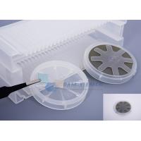
4H High Purity Semi Insulating SiC Wafer, Dummy Grade,3”Size
PAM-XIAMEN offers semiconductor silicon carbide wafers,6H SiC and 4H SiC in different quality grades for researcher and industry manufacturers. We has developed SiC crystal growth technology and SiC crystal wafer processing technology,established a production line to manufacturer SiCsubstrate,Which is applied in GaNepitaxydevice,powerdevices,high-temperature device and optoelectronic Devices. As a professional company invested by the leading manufacturers from the fields of advanced and high-tech material research and state institutes and China’s Semiconductor Lab,weare devoted to continuously improve the quality of currently substrates and develop large size substrates.
Here shows detail specification
SILICON CARBIDE MATERIAL PROPERTIES
| Polytype | Single Crystal 4H | Single Crystal 6H |
| Lattice Parameters | a=3.076 Å | a=3.073 Å |
| c=10.053 Å | c=15.117 Å | |
| Stacking Sequence | ABCB | ABCACB |
| Band-gap | 3.26 eV | 3.03 eV |
| Density | 3.21 · 103 kg/m3 | 3.21 · 103 kg/m3 |
| Therm. Expansion Coefficient | 4-5×10⁻⁶/K | 4-5×10⁻⁶/K |
| Refraction Index | no = 2.719 | no = 2.707 |
| ne = 2.777 | ne = 2.755 | |
| Dielectric Constant | 9.6 | 9.66 |
| Thermal Conductivity | 490 W/mK | 490 W/mK |
| Break-Down Electrical Field | 2-4 · 108 V/m | 2-4 · 108 V/m |
| Saturation Drift Velocity | 2.0 · 105 m/s | 2.0 · 105 m/s |
| Electron Mobility | 800 cm2/V·S | 400 cm2/V·S |
| hole Mobility | 115 cm2/V·S | 90 cm2/V·S |
| Mohs Hardness | ~9 | ~9 |
4H High Purity Semi Insulating SiC Wafer, Dummy Grade,3”Size
| SUBSTRATE PROPERTY | S4H-51-SI-PWAM-250 S4H-51-SI-PWAM-330 S4H-51-SI-PWAM-430 |
| Description | Dummy Grade 4H SEMI Substrate |
| Polytype | 4H |
| Diameter | (50.8 ± 0.38) mm |
| Thickness | (250 ± 25) μm (330 ± 25) μm (430 ± 25) μm |
| Resistivity (RT) | >1E5 Ω·cm |
| Surface Roughness | < 0.5 nm (Si-face CMP Epi-ready); <1 nm (C- face Optical polish) |
| FWHM | <50 arcsec |
| Micropipe Density | A+≤1cm-2 A≤10cm-2 B≤30cm-2 C≤50cm-2 D≤100cm-2 |
| Surface Orientation | |
| On axis <0001>± 0.5° | |
| Off axis 3.5° toward <11-20>± 0.5° | |
| Primary flat orientation | Parallel {1-100} ± 5° |
| Primary flat length | 16.00 ± 1.70 mm |
| Secondary flat orientation Si-face:90° cw. from orientation flat ± 5° | |
| C-face:90° ccw. from orientation flat ± 5° | |
| Secondary flat length | 8.00 ± 1.70 mm |
| Surface Finish | Single or double face polished |
| Packaging | Single wafer box or multi wafer box |
| Usable area | ≥ 90 % |
| Edge exclusion | 1 mm |
SiC Crystal Structure
SiC Crystal has many different crystal structures,which is called polytypes.The most common polytypes of SiC presently being developed for electronics are the cubic 3C-SiC, the hexagonal 4H-SiC and 6H-SiC, and the rhombohedral 15R-SiC. These polytypes are characterized by the stacking sequence of the biatom layers of the SiC structure.For more details, please enquire our engineer team.
Growth of Hexagonal Polytype SiC Wafers
In the late 1970s, Tairov and Tzvetkov established the basic principles of a modified seeded sublimation growth process for growth of 6H-SiC. This process, also referred to as the modified Lely process,was a breakthrough for SiC in that it offered the first possibility of reproducibly growing acceptably large single crystals of SiC that could be cut and polished into mass-produced SiC wafers. The basic growth process is based on heating polycrystalline SiC source material to ~2400°C under conditions, where it sublimes into the vapor phase and subsequently condenses onto a cooler SiC seed crystal .This produces a somewhat cylindrical boule of single-crystal SiC that grows taller roughly at the rate of a few millimeters per hour. To date, the preferred orientation of the growth in the sublimation process is such that vertical growth of a taller cylindrical boule proceeds along the <0 0 0 1> crystallographic c-axis direction (i.e., vertical direction in Fig. 5.1). Circular “c-axis” wafers with surfaces that lie normal (i.e., perpendicular to within 10°) to the c-axis can be sawed from the roughly cylindrical boule. After years of further development of the sublimation growth process, Cree, Inc., became the first company to sell 2.5 cm diameter semiconductor wafers of c-axis-oriented 6H-SiC in 1989. Correspondingly, the vast majority of SiC semiconductor electronics development and commercialization has taken place since 1990 using c-axis-oriented SiC wafers of the 6H and 4H-SiC polytypes. N-type, p-type, and semiinsulating SiC wafers of various sizes (presently as large as 7.6 cm in diameter) are now commercially available from a variety of vendors . It is worth noting that attainable substrate conductivities for p-type SiC wafers are more than 10× smaller than for n-type substrates, which is largely due to the difference between donor and acceptor dopant ionization energies in SiC (Table 5.1). More recently, SiC wafers grown with gas sources instead of sublimation of solid sources or a combination of gas and solid sources have also been commercialized . Growth of SiC boules and wafers oriented along other crystallographic directions, such as and “a-face” orientations, have also been investigated over the last decade . While these other SiC wafer orientations offer some interesting differences in device properties compared to conventional c-axis-oriented wafers (mentioned briefly in Section 5.5.5), all commercial SiC electronic parts produced (as of this writing) are manufactured using c-axis-oriented wafers.
Wafer size, cost, and quality are all very critical to the manufacturability and process yield of massproduced semiconductor microelectronics. Compared to commonplace silicon wafer standards, presentday 4H- and 6H-SiC wafers are smaller, more expensive, and generally of inferior quality containing far


