

Active Member
|
[China]

Address: #506B, Henghui Business Center, No.77, Lingxia Nan Road, High Technology Zone, Huli, Xiamen 361006, China
Contact name:

XIAMEN POWERWAY ADVANCED MATERIAL CO., LTD. |
|
|
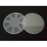
PAM-XIAMEN offers Compound Semiconductor GaSb wafer – gallium antimonide which are grown by LEC(Liquid Encapsulated Czochralski) as epi-ready or mechanical grade with n type, p type or semi-insulating in different orientation(111)or(100).
Gallium antimonide (GaSb) is a semiconducting compound of gallium and antimony of the III-V family.It has a lattice constant of about 0.61 nm. GaSb can be used for Infrared detectors,infrared LEDs and lasers and transistors, and thermophotovoltaic systems.
Here is the detail specification:
2″(50.8mm)GaSb Wafer Specification
3″(50.8mm)GaSb Wafer Specification
4″(100mm) GaSb Wafer Specification
2″ GaSb Wafer Specification
| Item | Specifications | ||
| Dopant | Undoped | Zinc | Tellurium |
| Conduction Type | P-type | P-type | N-type |
| Wafer Diameter | 2″ | ||
| Wafer Orientation | (100)±0.5° | ||
| Wafer Thickness | 500±25um | ||
| Primary Flat Length | 16±2mm | ||
| Secondary Flat Length | 8±1mm | ||
| Carrier Concentration | (1-2)x1017cm-3 | (5-100)x1017cm-3 | (1-20)x1017cm-3 |
| Mobility | 600-700cm2/V.s | 200-500cm2/V.s | 2000-3500cm2/V.s |
| EPD | <2×103cm-2 | ||
| TTV | <10um | ||
| BOW | <10um | ||
| WARP | <12um | ||
| Laser Marking | upon request | ||
| Suface Finish | P/E, P/P | ||
| Epi Ready | yes | ||
| Package | Single wafer container or cassette | ||
3″ GaSb Wafer Specification
| Item | Specifications | ||
| Conduction Type | P-type | P-type | N-type |
| Dopant | Undoped | Zinc | Tellurium |
| Wafer Diameter | 3″ | ||
| Wafer Orientation | (100)±0.5° | ||
| Wafer Thickness | 600±25um | ||
| Primary Flat Length | 22±2mm | ||
| Secondary Flat Length | 11±1mm | ||
| Carrier Concentration | (1-2)x1017cm-3 | (5-100)x1017cm-3 | (1-20)x1017cm-3 |
| Mobility | 600-700cm2/V.s | 200-500cm2/V.s | 2000-3500cm2/V.s |
| EPD | <2×103cm-2 | ||
| TTV | <12um | ||
| BOW | <12um | ||
| WARP | <15um | ||
| Laser marking | upon request | ||
| Suface finish | P/E, P/P | ||
| Epi ready | yes | ||
| Package | Single wafer container or cassette | ||
4″ GaSb Wafer Specification
| Item | Specifications | ||
| Dopant | Undoped | Zinc | Tellurium |
| Conduction Type | P-type | P-type | N-type |
| Wafer Diameter | 4″ | ||
| Wafer Orientation | (100)±0.5° | ||
| Wafer Thickness | 800±25um | ||
| Primary Flat Length | 32.5±2.5mm | ||
| Secondary Flat Length | 18±1mm | ||
| Carrier Concentration | (1-2)x1017cm-3 | (5-100)x1017cm-3 | (1-20)x1017cm-3 |
| Mobility | 600-700cm2/V.s | 200-500cm2/V.s | 2000-3500cm2/V.s |
| EPD | <2×103cm-2 | ||
| TTV | <15um | ||
| BOW | <15um | ||
| WARP | <20um | ||
| Laser marking | upon request | ||
| Suface finish | P/E, P/P | ||
| Epi ready | yes | ||
| Package | Single wafer container or cassette | ||
1)2″(50.8mm),3″(76.2mm)GaSb wafer
Orientation:(100)±0.5°
Thickness(μm):500±25;600±25
Type/Dopant:P/undoped;P/Si;P/Zn
Nc(cm-3):(1~2)E17
Mobility(cm2/V ·s):600~700
Growth Method:CZ
Polish:SSP
2)2″(50.8mm)GaSb wafer
Orientation:(100)±0.5°
Thickness(μm):500±25;600±25
Type/Dopant:N/undoped;P/Te
Nc(cm-3):(1~5)E17
Mobility(cm2/V ·s):2500~3500
Growth Method:LEC
Polish:SSP
3)2″(50.8mm)GaSb wafer
Orientation:(111)A±0.5°
Thickness(μm):500±25
Type/Dopant:N/Te;P/Zn
Nc(cm-3):(1~5)E17
Mobility(cm2/V ·s):2500~3500;200~500
Growth Method:LEC
Polish:SSP
4)2″(50.8mm)GaSb wafer
Orientation:(111)B±0.5°
Thickness(μm):500±25;450±25
Type/Dopant:N/Te;P/Zn
Nc(cm-3):(1~5)E17
Mobility(cm2/V ·s):2500~3500;200~500
Growth Method:LEC
Polish:SSP
5)2″(50.8mm)GaSb wafer
Orientation:(111)B 2deg.off
Thickness(μm):500±25
Type/Dopant:N/Te;P/Zn
Nc(cm-3):(1~5)E17
Mobility(cm2/V ·s):2500~3500;200~500
Growth Method:LEC
Polish:SSP
Relative products:
InAs wafer
InSb wafer
InP wafer
GaAs wafer
GaSb wafer
GaP wafer
Gallium Antimonide (GaSb) can be supplied as wafers with as-cut, etched or polished finishes and are available in a wide range of carrier concentration, diameter and thickness.
GaSb material presents interesting properties for single junction thermophotovoltaic (TPV) devices. GaSb: Te single crystal grown with Czochralski (Cz) or modified Czo- chralski (Mo-Cz) methods are presented and the problem of Te homogeneity discussed. As the carrier mobility is one of the key points for the bulk crystal, Hall measurements are carried out. We present here some complementary developments based on the material processing point of view: the bulk crystal growth, the wafer preparation, and the wafer etching. Subsequent steps after these are related to the p / no r n/p junction elaboration. Some results obtained for different thin-layer elaboration approaches are presented. So from the simple vapor phase diffusion process or the liquid phase epitaxy process up to the metal organic chemical vapor deposition process we report some material specificity.


