|
|
[China]

Trade Verify
Address: Address:Room624,Fangdichan development building,Guicheng south,Nanhai,Foshan,China
Contact name:Tracy

ONESEINE TECHNOLOGY CO.,LTD |
|
Verified Suppliers
|

|
|
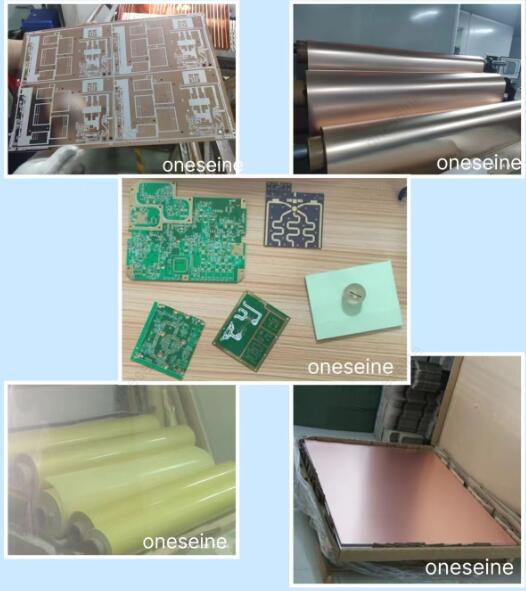
PTFE High Frequency Teflon 2 Layer Black OSP F4B PCB Board
PCB details:
Material | F4bM | Copper | 1OZ |
Layer | 2 | Size | 2*3CM |
Surface finish | OSP | Solder mask | Black |
Thickness | 1.6mm | Min line | 5mil |
F4B-1/2 is laminated with excellent material according to the
requirements of microwave circuit in electrical performance. It is
a kind of laminate of microwave PCB due to its excellent electrical
performance and higher mechanical strength.
Teflon woven glass fabric copper-clad laminates with high
permittivity
F4BK-1/2
F4BK-1/2 is laminated by laying up of varnished glass cloth with
Teflon resin, according to the scientific formulation and strict
technology process. This product takes some advantages over F4B
series in the electrical performance(wider range of dielectric
constant).
Teflon woven glass fabric copper-clad laminates with high
permittivity
F4BM-1/2
F4BM-1/2 is laminated by laying up of varnished glass cloth with
Teflon resin, according to the scientific formulation and strict
technology process. This product takes some advantages over F4B
series in the electrical performance(wider range of dielectric
constant,lower dielectric loss angle tangent,increased
resistance,and more stability of performance).
Teflon woven glass fabric copper-clad laminates with high
permittivity
F4BMX-1/2
F4BMX-1/2 is laminated by laying up of varnished glass cloth with
Teflon resin, according to the scientific formulation and strict
technology process. This product takes some advantages over F4B
series in the electrical performance(wider range of dielectric
constant,lower dielectric loss angle tangent,increased
resistance,and more stability of performance).Compared with the
F4BM,the consistency of the laminate various properties can be
insured through using the imported woven glass fabric.
Teflon woven glass fabric copper-clad laminates with high
permittivity
F4BME-1/2
F4BME-1/2 is laminated by laying up of the imported varnished glass
cloth with Teflon resin,according to the scientific formulation and
strict technology process. This product takes some advantages over
F4BM series in the electrical performance and the passive
intermodulation indicators increased.
Teflon woven glass fabric copper-clad laminates with ceramic filled
F4BT-1/2
F4BT-1/2 is a micro dispersed ceramic PTFE composite with a woven
fiberglass reinforcement through scientific formulation and strict
technology procedures. This product have higher dielectric constant
than the traditional PTFE copper clad laminates to meet the design
and manufacturing of circuit miniaturization. Due to filling with
the ceramic powder,F4BT-1/2have a low Z axis coefficient of thermal
expansion ensures excellent reliability of plated through-holes.
Besides,because of the high thermal conductivity,advantage to the
heat dissipation of apparatus.
F4BDZ294
1.Introduction:
F4BDZ294 is a kind of Teflon woven glass fabric planar resistor
copper-clad laminates with the dielectric constant of 2.94. This
kind of high frequency laminates is manufactured by Teflon woven
glass fabric(with low dielectric constant and low dissipation
factor)with the planar resistor copper foil. It features with
excellent electrical and mechanical performance. Its high
mechanical reliability and excellent electrical stability is
suitable for the design of the complicated microwave circuit.
Structure of the material:One side is clad with resistor copper
foil,and the other side is clad with traditional copper foil,and
the dielectric material with Teflon woven glass fabric. The
dielectric constant is 2.94.
Features of the material:low dielectric constant and loss;excellent
electrical / mechanical performance;lower thermal coefficient of
dielectric constant;low outgassing.
2.Application scope
(1)Ground-based and airborne radar system;
(2)Phased array antenna;
(3)GPS antenna;
(4)Power backboard;
(5)Multilayer PCB;
(6)Spotlight network.
Metal base Teflon woven glass fabric copper-clad laminates
F4B-1/AL(Cu)
F4B-1/AL(Cu) is a kind of microwave circuit metal base material
based on Teflon woven glass fabric copper-clad laminates,which is
pressed with copper on one side,and aluminum(copper)plate on the
other side.
Teflon copper-clad laminates
F4T-1/2
F4T-1/2 is a kind of circuit laminate based on the Teflon
board,which is compressed with electrolytic copper foil(after
oxidation treatment)on both sides,and then pressed together after
high temperature and high pressure. This product takes some
advantages in the electrical performance(low dielectric
constant,low dielectric loss angle tangent). It is a good kind of
laminate of microwave PCB due to its higher mechanical strength.
Microwave composite dielectric copper-clad substrate
TP-1/2
The advantage of design for microwave circuit using TP-1/2 here:
(1)The dielectric constant is stable and can be optional within the
range of 3~16 according to the design of circuit requirement. The
operating temperature is -100℃~+150℃;
(2)The peel strength between the copper and the substrate is more
reliable than the vacuum film coating of ceramic substrate. This
substrate is created to offer customers easy for circuit
processing,higher pass-rate of production,and the manufacturing
cost is much lower than the ceramic substrate.
(3)Dissipation factor tgδ≤1×10⁻³,and the loss has a slight
variation with the rise of the frequency.
(4)It is easy for mechanical manufacturing,including
drill,punch,grind,cut,etching,etc.. For these,the ceramic substrate
cannot be compared.
A special microwave composite dielectric copper-clad substrate
TPH-1/2
TPH-1/2 is made of a new type of inorganic and organic
materials,with special process and compounding.
The advantage of design for microwave circuit using TPH-1/2 here:
(1)The substrate is black. The dielectric constant is 2.65,with
consistent performance over broad temperature and frequency ranges.
The operating temperature is -100℃~+150℃;
(2)The peel strength between the copper and the substrate is more
reliable than the vacuum film coating of ceramic substrate. This
substrate is created to offer customers easy for circuit
processing,higher pass-rate of production,and the manufacturing
cost is much lower than the ceramic substrate.
(3)Dissipation factor tgδ≤1×10⁻³,and the loss has a slight
variation with the rise of the frequency.
(4)It is easy for mechanical manufacturing,including
drill,punch,grind,cut,etching,etc.. For these,the ceramic substrate
cannot be compared.
(5) Due to the specific gravity less,the remarkable characteristics
of the module are weight lighter manufacturing by this
substrate,which but other materials cant compare.
(6)Copper thickness is:0.035μm
Teflon ceramic composite dielectric substrate
TF-1/2
TF-1/2 is a kind of circuit laminate based on the Teflon(which have
excellent microwave and temperature resistance performance)compound
with ceramic. This kind of laminate can be comparable with the
products(such as RT/duroid 6006/6010/TMM10)from Rogers Corporation
in United State of America.
The advantage of design for microwave circuit using TF-1/2 here:
(1)The operating temperature is much higher than TP-series. It is
applicable to long-term operation within temperature ranger of
-80℃~+200℃,and can be used for wave-welding and melt-back welding.
(2)Used for the manufacturing of the microwave and millimeter wave
printed circuit board .
(3)Better radiation performance,30min20rad/cm2.
(4)Dielectric property is stable and has a slight variation with
the rise of temperature and frequency.
Teflon woven glass fabric
F4B-N / F4B-J / F4B-T
This product is the raw material for the Teflon woven glass fabric
copper-clad laminates. Dipping treatment of the Teflon resin on the
alkali-free woven glass fabric,drying,baking and sintering,the
microwave material is formulated. This product is characterized by
some features,such as heat-resistance,insulation,low loss,excellent
electrical performance,in-adhesion. The Teflon woven glass fabric
is Widely used in electronics,motor,aviation,textile,chemical and
food industry,etc.. In the area of microwave devices,it can be used
as the bond film for the manufacturing of multilayer printed
circuit board.
1.Type of material
(1)Anti-sticking Teflon woven glass fabric:F4B-N ;
(2)Insulation Teflon woven glass fabric:F4B-J ;
(3)Ventilated Teflon woven glass fabric:F4B-T .
High frequency PCB range:
Frequency Range: High-frequency PCBs are designed to operate in frequency ranges typically starting from a few megahertz (MHz) and extending into the gigahertz (GHz) and terahertz (THz) ranges. These PCBs are commonly used in applications such as wireless communication systems (e.g., cellular networks, Wi-Fi, Bluetooth), radar systems, satellite communication, and high-speed data transmission.
Signal Loss and Dispersion: At high frequencies, signal loss and dispersion become significant concerns. High-frequency PCBs employ techniques to minimize these effects, such as using low-loss dielectric materials, controlled impedance routing, and minimizing the length and number of vias.
PCB Stackup: The stackup configuration of a high-frequency PCB is carefully designed to address signal integrity requirements. It typically consists of multiple layers of copper traces, dielectric materials, and ground planes. The arrangement of these layers is optimized to control impedance, minimize crosstalk, and provide shielding.
RF Connectors: High-frequency PCBs often incorporate specialized RF connectors to ensure proper signal transmission and minimize losses. These connectors are designed to maintain consistent impedance and minimize reflections.
Electromagnetic Compatibility (EMC): High-frequency PCBs must comply with electromagnetic compatibility standards to prevent interference with other electronic devices and to avoid susceptibility to external interference. Proper grounding, shielding, and filtering techniques are employed to address EMC requirements.
Simulation and Analysis: Designing high-frequency PCBs often involves simulation and analysis using specialized software tools. These tools allow designers to assess signal integrity, impedance matching, and electromagnetic behavior before fabrication, helping to optimize the PCB design for high-frequency performance.
Fabrication Challenges: Fabricating high-frequency PCBs can be more challenging compared to standard PCBs. The use of specialized materials, controlled impedance requirements, and tight tolerances require advanced fabrication techniques such as accurate etching, controlled dielectric thickness, and precise drilling and plating processes.
Testing and Validation: High-frequency PCBs undergo rigorous testing and validation to ensure their performance meets the desired specifications. This includes impedance testing, signal integrity analysis, insertion loss measurement, and other RF and microwave tests.
It's important to note that the design and manufacturing of high-frequency PCBs are specialized areas requiring expertise in RF and microwave engineering, PCB layout, and fabrication processes. Working with experienced professionals and consulting relevant design guidelines and standards is crucial to ensure reliable performance at high frequencies.
High frequency PCB description:
High frequency PCB material in stock:
| Brand | Model | Thickness(mm) | DK(ER) |
| Rogers | RO4003C | 0.203mm,0.305mm,0.406mm,0.508mm,0.813mm,1.524mm | 3.38 ± 0.05 |
| RO4350B | 0.101mm,0.168mm,0.254mm,0.338mm,0.422mm,0.508mm,0.762mm,1.524mm | 3.48 ± 0.05 | |
| RO4360G2 | 0.203mm,0.305mm,0.406mm,0.508mm,0.610mm,0.813mm,1.524mm | 6.15 ± 0.15 | |
| RO4835 | 0.168mm,0.254mm,0.338mm,0.422mm,0.508mm,0.591mm, 0.676mm,0.762mm,1.524mm | 3.48 ± 0.05 | |
| RT5870 | 0.127mm,0.787mm,0.254mm,1.575mm,0.381mm,3.175mm,0.508mm | 2.33 2.33 ± 0.02 | |
| RT5880 | 0.127mm,0.787mm,0.254mm,1.575mm,0.381mm,3.175mm,0.508mm | 2.20 2.20 ± 0.02 | |
| RO3003 | 0.13mm,0.25mm,0.50mm,0.75mm,1.52mm | 3.00 ±0.04 | |
| RO3010 | 0.13mm,0.25mm,0.64mm,1.28mm | 10.2 ± 0.30 | |
| RO3006 | 0.13mm,0.25mm,0.64mm,1.28mm | 6.15 ± 0.15 | |
| RO3203 | 0.25mm,0.50mm,0.75mm,1.52mm | 3.02±0.04 | |
| RO3210 | 0.64mm,1.28mm | 10.2±0.50 | |
| RO3206 | 0.64mm,1.28mm | 6.15±0.15 | |
| R03035 | 0.13mm,0.25mm,0.50mm,0.75mm,1.52mm | 3.50 ± 0.05 | |
| RT6002 | 0.127mm,0.254mm,0.508mm,0.762mm,1.524mm,3.048mm | 2.94 ± 0.04 | |
| RT6006 | 0.127mm,0.254mm,0.635mm,1.27mm,1.90mm,2.50mm | 6.15± 0.15 | |
| RT6010 | 0.127mm,0.254mm,0.635mm,1.27mm,1.90mm,2.50mm | 10.2 ± 0.25 | |
| TACONIC | TLX-8.TLX-9 | 0.508. 0.762 | 2.45-2.65 |
| TLC-32 | 0.254,0.508,0.762 | 3.35 | |
| TLY-5 | 0.254,0.508.0.8, | 2.2 | |
| RF-60A | 0.254.0.508.0.762 | 6.15 | |
| CER-10 | 0.254.0.508.0.762 | 10 | |
| RF-30 | 0.254.0.508.0.762 | 3 | |
| TLA-35 | 0.8 | 3.2 | |
| ARLON | AD255C06099C | 1.5 | 2.55 |
| MCG0300CG | 0.8 | 3.7 | |
| AD0300C | 0.8 | 3 | |
| AD255C03099C | 0.8 | 2.55 | |
| AD255C04099C | 1 | 2.55 | |
| DLC220 | 1 | 2.2 |