
|
|
[China]

Trade Verify
Address: Address:Room624,Fangdichan development building,Guicheng south,Nanhai,Foshan,China
Contact name:Tracy

ONESEINE TECHNOLOGY CO.,LTD |
|
Verified Suppliers
|
|
|
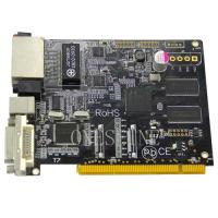
OEM One Stop Electronic SMT / DIP PCBA Assembly Control Circuit Boards
General information:
Layer:2
Material:Fr4
Board thickness:1.0mm
Copper weight:1OZ
Solder mask:Green
White silkscreen:White
Min line:5mil
Min hole:0.3mm
Name:SMT / DIP PCBA Assembly Control Circuit Boards
Application:Computer,communication field
SMT / DIP PCBA control circuit boards Manufacturer
a) Components sourcing
Common components are replaced to be High Quality China brand componnets at the condition of permission,
Decreasing cost for clients is one part of our jobs.
Genuine components are ordered from your designated supplier or our partner companies including Digikey,Mouser,
Arrow, Avnet,Future Electronic,Farnell,etc.
b) Type of assembly
SMT and Thru-hole
c) Assembly capacity
Stencil size/range : 736 × 736mm
Minimum IC pitch : 0.30mm
Maximum PCB size : 410 × 360mm
Minimum PCB thickness : 0.35mm
Minimum chip size : 0201 (0.2 × 0.1)/0603 (0.6 x 0.3mm)
Maximum BGA size : 74 × 74mm
BGA ball pitch : 1.00mm (minimum), 3.00mm (maximum)
BGA ball diameter : 0.40mm (minimum), 1.00mm (maximum)
QFP lead pitch : 0.38mm (minimum), 2.54mm (maximum)
Frequency of stencil cleaning : 1 time/5 to 10 pieces
The PCB assembly process typically includes the following steps:
Component Procurement: The required electronic components are sourced from suppliers. This involves selecting components based on specifications, availability, and cost.
PCB Fabrication: The bare PCBs are manufactured using specialized techniques such as etching or printing. The PCBs are designed with copper traces and pads to establish electrical connections between the components.
Component Placement: Automated machines, called pick-and-place machines, are used to accurately place surface mount components (SMD components) on the PCB. These machines can handle a large number of components with precision and speed.
Soldering: Once the components are placed on the PCB, soldering is performed to establish electrical and mechanical connections. There are two common methods used for soldering: a. Reflow Soldering: This method involves applying solder paste to the PCB, which contains small solder balls. The PCB is then heated in a reflow oven, causing the solder to melt and create connections between the components and the PCB. b. Wave Soldering: This method is typically used for through-hole components. The PCB is passed over a wave of molten solder, which creates solder connections on the bottom side of the board.
Inspection and Testing: After soldering, the assembled PCBs undergo inspection to check for defects, such as solder bridges or missing components. Automated optical inspection (AOI) machines or human inspectors perform this step. Functional testing may also be conducted to ensure the PCB operates as intended.
Final Assembly: Once the PCBs pass inspection and testing, they can be integrated into the final product. This may involve additional assembly steps, such as attaching connectors, cables, enclosures, or other mechanical components.
Certainly! Here are some additional details about PCB assembly:
Surface Mount Technology (SMT): Surface mount components, also known as SMD (Surface Mount Device) components, are widely used in modern PCB assembly. These components have small footprints and are mounted directly onto the surface of the PCB. This allows for higher component density and smaller PCB sizes. SMT components are typically placed using automated pick-and-place machines, which can handle components of various sizes and shapes.
Through-Hole Technology (THT): Through-hole components have leads that pass through holes in the PCB and are soldered on the opposite side. While SMT components dominate modern PCB assembly, through-hole components are still used for certain applications, especially when components require extra mechanical strength or high power handling capabilities. Wave soldering is commonly used for soldering through-hole components.
Mixed Technology Assembly: Many PCBs incorporate a combination of surface mount and through-hole components, referred to as mixed technology assembly. This allows for a balance between component density and mechanical strength, as well as accommodating components that are not available in surface mount packages.
Prototype vs. Mass Production: PCB assembly can be performed for both prototype and mass production runs. In prototype assembly, the focus is on building a small number of boards for testing and validation purposes. This may involve manual component placement and soldering techniques. Mass production, on the other hand, requires high-speed automated assembly processes to achieve efficient and cost-effective production of large quantities of PCBs.
Design for Manufacturing (DFM): DFM principles are applied during the PCB design phase to optimize the assembly process. Design considerations such as component placement, orientation, and proper clearances help ensure efficient assembly, reduce manufacturing defects, and minimize production costs.
Quality Control: Quality control is an integral part of PCB assembly. Various inspection techniques are employed, including visual inspection, automated optical inspection (AOI), and X-ray inspection, to detect defects such as solder bridges, missing components, or incorrect orientations. Functional testing may also be conducted to verify the proper operation of the assembled PCB.
RoHS Compliance: Restriction of Hazardous Substances (RoHS) directives restrict the use of certain hazardous materials, such as lead, in electronic products. PCB assembly processes have adapted to comply with RoHS regulations, using lead-free soldering techniques and components.
Outsourcing: PCB assembly can be outsourced to specialized contract manufacturers (CMs) or electronic manufacturing service (EMS) providers. Outsourcing allows companies to leverage the expertise and infrastructure of dedicated assembly facilities, which can help reduce costs, increase production capacity, and access specialized equipment or expertise.
PCB Assembly (PCBA) Process:
Step 1: Applying Solder Paste Using Stencil
First of all we apply the solder paste on the areas of the printed circuit board assemblies where the components will fit. This is done by applying solder paste on the stainless steel stencil. The stencil and the PCB are hold together by a mechanical fixture and then the solder paste is applied by the applicator evenly to all opening in the board. The applicator spreads the solder paste equally. So a right amount of solder paste must be used in applicator. When the applicator is removed the paste will remain in the desired areas of PCB. The grey color solder paste is 96.5% made of tin and contains 3% of silver and 0.5% of copper and it is lead free. This solder paste will melt and creates a strong joint upon application of heat in step 3.
Step 2: Automated Placement of Components:
The second step in pcba is the automated placement of SMT components on PCB board. This is done by using pick and place robot. At the design level the designer creates a file that will be fed to the automated robot. This file has the preprogrammed X,Y coordinates of each and every components used in PCB and it identifies the location of all components. Using this information the robot will simply place the SMD devices on board accurately. The pick and place robots will pick the components from its vacuum grip and place exactly on top of solder paste.
Before the advent of robotic pick and place machines, the technician will pick the components using tweezers and place it on PCB by carefully looking at the location and avoiding any jittering hands. This resulted in high level of fatigue and eyesight weakness in technicians and resulted in slowed process of PCB assembly of SMT components. Hence the chances of mistake were high.
As the technology matured, automated robots for pick and place components eased the technicians work and resulted in fast and accurate components placement. These robots can work 24/7 without fatigue.
Step 3: Reflow Soldering
The third step after the components are set and solder paste applied is reflow soldering. The reflow soldering is the process where the PCBs along with the components are put on the conveyer belt. This conveyer belt then moves the PCBs and components in a big oven, which creates a temperature of 250o C. This temperature is enough for the solder to melt. The melted solder will then fix the components upon the PCB and create joints. After the PCB is treated with high temperature, it then goes in to coolers. These coolers then solidifies the solder joints in controlled fashion. This will create a permanent joint between SMT component and PCB. In the case of two sided PCBs, the PCB side which has fewer or smaller components will be treated first from step 1 to 3 as mentioned above and then comes the other side.
Step 4: QC and Inspection
After the reflow soldering, there is a chance that due to some erroneous movement in PCB holding tray, the components got misaligned and may result in short circuit or open connection. These flaws are need to be identified and this identification process is called inspection. Inspection can be manual and automated.
a. Manual Inspection:
As the PCB has the small SMT components, so visually checking the board for any misalignment or faults can result in fatigue and eye strains for technicians. So this method is not feasible for advance SMT boards due to inaccurate results. However this method is feasible for boards having THT components and lesser components density.
b. Optical Inspection:
For the large batches of PCB, this method is feasible. This method uses the automated machine that has the high powered and high resolution cameras installed at various angles to view the solder joints from various directions. The light will reflect the solder joints in different angles according to the quality of solder joints. This automated Optical Inspection (AOI) machine is very high speed and take very short time to process large batches of PCBs.
c.X-ray Inspection:
The X-Ray machine allows the technician to look through the PCB to see the inner layer defects. This is not a common inspection method and is only used in complex and advance PCBs. These inspection methods if not properly applied may cause rework or scrap PCB. The inspection need be done regular basis to avoid delays, labor and material cost.
Step 5: THT Component Fixation and Soldering
The through-hole components are commonly found on many PCB boards. These components are also known as Plated through Hole (PTH). These components have leads that will pass through the hole in the PCB. These holes connect to other holes and vias by means of copper traces. When these THT components are inserted and soldered in these holes, then they are electrically connected to other hole in the same PCB as the circuit designed. These PCBs may contain some THT components and many SMD components so the soldering method as discussed above in case of SMT components like reflow soldering will not work on THT components.
a. Manual Soldering:
The manual soldering method is the common and typically takes more time than compared to automated setup for SMT. Usually one technician is designated to insert one component at a time and the board is passed on to other technician who inserts another component on the same board. So the board will move all around the assembly line to get the PTH components stuffed upon it. This makes the process lengthy and so many PCB design and manufacturing companies avoid using PTH components in their circuit design. But still the PTH components are the most favorite and common components for most of the circuit designers.
b. Wave Soldering:
The automated version of manual soldering is wave soldering. In this method, once the PTH components are placed on the PCB, the PCB is put on the conveyer belt and is moved to specialized oven. Here a wave of molten solder is splashed on the PCB bottom layer where the components leads are present. This will solder all the pins at once. However this method is only for single sided PCBs and not for double sided because this molten solder while soldering one side of PCB can damage components on other side. After this, the pcb fabrication and assembly is moved for final inspection.
Step 6: Final Inspection and Functional Test
Now the PCB is ready for testing and inspection. This is the functionality test, where electrical signals and power supply is given to the PCB at the specified pins and output is checked at the specified test points or output connectors. This test requires common lab instruments like oscilloscope, DMM, function generator
This test is to check the functionality and electrical characteristics of PCB and to verify current, voltage, analog and digital signals as described in the requirements of PCB and circuit design
If any of the parameters of the PCB shows unacceptable results, then the PCB is discarded or scrapped as per the company standard procedures. Testing phase is very important because it determines the success or failure of the entire process of PCBA.
Step 7: Final Cleaning, Finishing and Shipment:
Now that the PCB is tested and declared OK from all aspects, it is time now to clean the unwanted residual flux, finger dirt and oils stains. A stainless steel based high pressure washing tool using deionized water is sufficient to clean all types of dirt. The deionized water will not damage the PCB circuit. After washing the PCB is dried by compressed air. Now the final PCB is ready for pack up and shipment.


