
|
|
[China]

Trade Verify
Address: Address:Room624,Fangdichan development building,Guicheng south,Nanhai,Foshan,China
Contact name:Tracy

ONESEINE TECHNOLOGY CO.,LTD |
|
Verified Suppliers
|
|
|
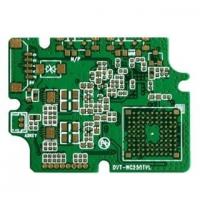
Switching Power Supply FR4 Custom Pcb Builder Thick Copper Printed Circuit Board
PCB information:
Number of layers: 2
Board thickness: 1.6+/-0.14MM+
Size: 274.81mm*216.64mm
Plate used: ITEQ (IT158)
Minimum aperture: 0.4mm
Surface treatment: lead-free spray tin
Spray tin thickness: 1um
Minimum line width/distance: 0.384mm/0.195mm
Customized pcb application:
The application of a customized PCB can vary widely depending on the specific requirements and purpose of the project. Here are some common applications where customized PCBs are used:
1,Consumer Electronics: Custom PCBs are widely used in various consumer electronic devices such as smartphones, tablets, laptops, gaming consoles, wearable devices, audio/video equipment, and home automation systems.
2,Industrial Automation: Customized PCBs find extensive application in industrial automation systems, including programmable logic controllers (PLCs), motor control systems, robotics, process control systems, and instrumentation.
3,Internet of Things (IoT): With the increasing popularity of IoT, customized PCBs play a crucial role in enabling connectivity and smart functionality in IoT devices such as sensors, actuators, gateways, and edge devices.
4,Automotive Electronics: Custom PCBs are used in various automotive applications, including engine control units (ECUs), infotainment systems, advanced driver assistance systems (ADAS), navigation systems, and lighting control modules.
5,Medical Devices: Customized PCBs are essential in medical devices such as patient monitoring systems, diagnostic equipment, imaging systems, implantable devices, and medical wearables.
6,Aerospace and Defense: PCBs designed for aerospace and defense applications require high reliability, ruggedness, and adherence to stringent quality standards. They are used in avionics systems, satellite communication systems, radar systems, and military equipment.
7,Renewable Energy: Customized PCBs are utilized in renewable energy systems such as solar inverters, wind turbine control systems, energy monitoring systems, and battery management systems.
8,Research and Development: Custom PCBs are often used in research and development projects across various domains, including prototyping of new electronic devices, experimental circuits, and proof-of-concept designs.
These are just a few examples, and the applications of customized PCBs are not limited to these areas. PCBs are a fundamental component in almost all electronic devices and systems, and customization allows for optimized performance, integration, and functionality tailored to specific requirements.
To design a customized PCB, you'll need to follow these general steps:
Schematic Design: Create a schematic diagram of your circuit using a PCB design software. This step involves selecting and connecting the desired components, such as microcontrollers, sensors, ICs, resistors, capacitors, etc. If you already have a schematic, you can skip this step.
PCB Layout Design: Once the schematic is complete, you'll need to create the physical layout of the PCB. This involves placing the components on the board and routing traces to connect them according to the schematic. Consider factors like component placement for optimal signal flow, power and ground planes, and any mechanical constraints.
Component Placement: Carefully place the components on the PCB layout, taking into account factors such as signal integrity, thermal management, and space constraints. Ensure proper clearances between components and adherence to design guidelines for each component.
Routing: Establish connections between components by routing traces on the PCB. Pay attention to signal integrity, impedance control, and avoiding signal crosstalk. Use appropriate trace widths, vias, and layer stack-up to meet your design requirements.
Design Rule Check (DRC): Run a design rule check to ensure your PCB layout complies with the fabrication and assembly constraints. This step helps identify errors or violations like clearance violations, unconnected nets, or overlapping components.
Gerber File Generation: Generate the necessary Gerber files from your PCB design software. These files contain the manufacturing information for the PCB, including copper layers, solder mask, silkscreen, drill files, and more.
PCB Fabrication: Send the Gerber files to a PCB manufacturer or fabricator to produce the physical PCB. Choose a manufacturer that suits your requirements in terms of quality, cost, and turnaround time. Provide them with any additional specifications such as material type, board thickness, surface finish, and quantity.
PCB Assembly: Once you receive the fabricated PCBs, you can proceed with the assembly stage. This involves soldering the components onto the PCB. You can either do it yourself if you have the necessary skills and equipment or outsource it to a PCB assembly service.
It's important to note that designing a customized PCB requires knowledge of electronics, PCB design principles, and proficiency in PCB design software. If you are new to PCB design, it may be helpful to consult with an experienced engineer or work with a professional PCB design service.
If you have any specific requirements or questions during the design process, feel free to ask for assistance.


