

Active Member
|
[China]

Address: Block 11, International E-Commerce Logistic Center, PingHu Street, LongGang Distric, ShenZhen City
Contact name:Steven

Witgain Technology Ltd |
|
|
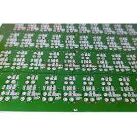
2 Layer Thick Copper PCB
PCB Specifications:
Layer Count: 2 Layer PCB
Material: FR4, IT180A
Board Thickness: 3.5MM
Min Hole: 0.3MM
Min Trace: 20/10Mil
Copper: 3/3OZ
Solder Mas: Green
Unit Size: 165MM*144MM/1pcs
Surface Treatment: HASL
Application: Power Supply
Capabilities:
| Item | Capability |
| Layer Count | 1-24 Layers |
| Board Thickness | 0.1mm-6.0mm |
| Finished Board Max Size | 700mm* 800mm |
| Finished Board Thickness Tolerance | +/-10% +/-0.1(<1.0mm) |
| Warp | <0.7% |
| Major CCL Brand | KB/NanYa/LTEQ/ShengYi/Rogers Etc |
| Material Type | FR4,CEM-1,CEM-3,Aluminum,Copper,Ceramic, PI, PET |
| Drill Hole Diameter | 0.1mm-6.5mm |
| Out Layer Copper Thickness | 1/20Z-8OZ ; |
| Inner Layer Copper Thickness | 1/3OZ-6OZ |
| Aspect Ratio | 10:1 |
| PTH Hole Tolerance | +/-3mil |
| NPTH Hole Tolerance | +/-1mil |
| Copper Thickness Of PTH Wall | >10mil(25um) |
| Line Width And Space | 2/2mil |
| Min Solder Mask Bridge | 2.5mil |
| Solder Mask Alignment Tolerance | +/-2mil |
| Dimension Tolerance | +/-4mil |
| Max Gold Thickness | 200u'(0.2mil) |
| Thermal Shock | 288C, 10s, 3 Times |
| Impedance Contro | +/-10% |
| LTest Capability | PAD Size Min 0.1mm |
| Min BGA | 7mil |
| Surface Treatment | OSP, ENIG, HASL, Plating Gold, Carbon Oil,Peelable |
FAQ:
Question: What is Loss Tangent?
Answer: In PCBs, Loss tangent (tan (δ)) is the measure of signal loss due to the inherent dissipation of electromagnetic energy in the substrate of the printed circuit board. It is a dimensionless quantity and generally referred to: Loss Factor, Tan δ, Dissipation factor and Loss angle.
All PCB materials have both conduction losses and dielectric losses. The conduction losses are resistive and are caused by the conductive copper layer used in the board. The dielectric losses on the other hand are associated with the substrate (insulating material) used in a PCB. When the electric field is applied, polarization occurs and charges are displaced relative to the electric field. Dielectric losses cause a reduction in the overall electric field.

The total amount of polarization that can occur in a dielectric depends upon the molecular symmetry of the insulator material and is called Dipole Moment. The effect of the dipole moment in a dielectric substrate is termed Loss Tangent.
Mathematically, the loss tangent is the phase angle between the resistive and reactive components of a system with permittivity. A low value of loss tangents results in a "fast" substrate while large value results in a "slow" substrate.

The formula for Loss Tangent or the Dissipation Factor is:

where δ is the loss angle, θ is the phase angle, f is the frequency, Rp is the equivalent parallel resistance, and Cp is the equivalent parallel capacitance.
The signal loss by the dielectric material depends upon the material’s structure and glass-resin composition. Selection of low loss materials is the major task for manufacturers that is why they are advised to plot the attenuation equation against frequency for various material choices.
Loss tangent plays a crucial factor for very high frequencies above 1 GHz and analog signals to determine the signal attenuation.
Quesion: What is the Solder Mask?
Answer: Solder mask or solder resist is a coating applied to a Printed Circuit Board (PCB) to protect the copper traces on the board and to stop electrical shorts. The solder mask is usually applied on both sides of the PCB i.e Top and Bottom to ensure reliability and performance.
The solder mask is a Liquid UV Photo-imageable Ink which is usually green in color. Other color options like red, blue, yellow, white, black and purple are also available. This is something you need to ask your PCB fabricator.
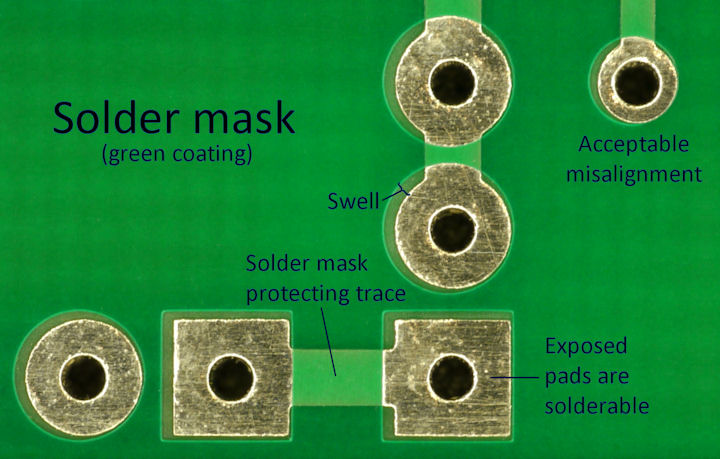
In the image above, the light green line is the solder mask layer. As you can see, the solder mask covers the entire trace, leaving only the pads exposed which are required to make electrical connections.
What is the purpose of using a solder mask?
What material is used for solder mask?
Resin is usually selected as the main material for solder mask because it works exceptionally well in terms of humidity resistance, insulation, solder resistance and high-temperature resistance.


