Active Member
|
[China]

Address: Huishang Building, 19-128 Nathan Road, Yau Tsim Sha Tsui, Yau Tsim, Hong Kong
Contact name:Mank.Li

Shenzhen Chaosheng Electronic Technology Co.,Ltd |
|
|
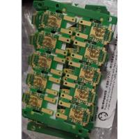
8 layers HD3 level, embedded copper PCB embedded embedded capacitance / buried resistance PCB Communication Network Optical Module PCB Power Optical Module PCB Wireless Optical Module PCB High Power Optical Module PCB
Product Description
Product Details
PCB, FPC process production capability
| Technical ltem | MassProduct | Advanced Technology | |||||
| 2016 | 2017 | 2018 | |||||
| Max.Layer Count | 26L | 36L | 80L | ||||
| Through-hole plate | 2~45L | 2~60L | 2~80L | ||||
| Max.PCBSize(in) | 24*52" | 25*62" | 25*78.75" | ||||
| The layer number of FPC | 1~36L | 1~50L | 1~60L | ||||
| Max.PCBSize(in) | 9.8"*196" | 9.8"*196" | 10"*196"Reel to reel | ||||
| Layeredplatelayer | 2~12L | 2~18L | 2~26L | ||||
| Max.PCBSize(in) | 9"*48" | 9"*52" | 9"*62" | ||||
| Combination of hard and soft layers | 3~26L | 3~30L | 3~50L | ||||
| Interconnect HDI | 5+X+5Interconnect HDI | 7+X+7Interconnect HDI | 8+X+8,Interconnect HDI | ||||
| HDI PCB | 4~45L | 4~60L | 4~80L | ||||
| Interconnect HDI | 3+20+3 | 4+X+4Interconnect HDI | 4+X+4,Interconnect HDI | ||||
| Max.PCBSize(in) | 24"*43" | 24"*49" | 25"*52" | ||||
| Material | FR-4 Rogers | FR-4 Rogers | FR-4 Rogers | ||||
| Base material | Halogenfree,LowDK | Halogenfree,LowDK | Halogenfree,LowDK | ||||
| Build-up Material | FR-4 | FR-4 | FR-4 | ||||
| BOard,Thickness(mm) | Min.12L(mm) | 0.43 | 0.42~8.0mm | 0.38~10.0mm | |||
| Min.16L(mm) | 0.53 | 1.60~8.0mm | 0.45~10.0mm | ||||
| Min.18L(mm) | 0.63 | 2.0~8.0 | 0.51~10.0mm | ||||
| Min.52L(mm) | 0.8 | 2.50~8.0mm | 0.65~10.0mm | ||||
| MAX(mm) | 3.5 | 10.0mm | 10.0mm | ||||
| Min.CoreThickness um(mil) | 254"(10.0) | 254"(10.0) | 0.10~254(10.0mm) | ||||
| Min.Build up Dielectric | 38(1.5) | 32(1.3) | 25(1.0) | ||||
| BaseCopperWeight | Inner Layer | 4/1-8 OZ | 4/1-15 OZ | 4/1-0.30mm | |||
| Out Layer | 4/1-10 OZ | 4/1-15 OZ | 4/1-30 OZ | ||||
| Gold thick | 1~40u" | 1~60u" | 1~120u" | ||||
| Nithick | 76~127u" | 76~200u" | 1~250u" | ||||
| Min.HOle/Land um(mil) | 150/300(6/12) | 100/200(4/8) | 100/200(4/8) | ||||
| Min.Laser via/landum(mil) | 60/170(2.4/6.8) | 50/150(2/6) | 50/150(2/6) | ||||
| Min. IVH,Hole size/landum(mil) | 150/300(6/12) | 100/200(4/8) | 100/200(4/8) | ||||
| DieletricThickness | 38(1.5) | 32(1.3) | 32(1.3) | ||||
| 125(5) | 125(5) | 125(5) | |||||
| SKipvia | Yes | Yes | Yes | ||||
| viaoNhie(laserviaon BuriedPTH) | Yes | Yes | Yes | ||||
| Laser Hole Filling | Yes | Yes | Yes | ||||
| Technicalltem | Mass Product | Advanced Technolgy | |||||
| 2017year | 2018year | 2019year | |||||
| Drill hole depth ratio | ThroughHole | 2017year | .40:1 | .40:1 | |||
| Aspet Ratio | Micro Via | .35:1 | 1.2:1 | 1.2:1 | |||
| Copper Filling Dimple Size um(Mil) | 10(0.4) | 10(0.4) | 10(0.4) | ||||
| Min.LineWidth&space | lnner Layer um(mil) | 45/45(1.8/1.8) | 38/38(1.5/1.5) | 38/38(1.5/1.5) | |||
| Plated Layer um(mil) | 45/45(1.8/1.8) | 38/38(1.5/1.5) | 38/38(1.5/1.5) | ||||
| BGAPitch mm(Mil) | 0.3 | 0.3 | 0.3 | ||||
| Min.PTH Hole ring um(mil) | 75(3mil) | 62.5(2.5mil) | 62.5(2.5mil) | ||||
| Line Width Control | ∠2.5MIL | ±0.50 | ±0.50 | ±0.50 | |||
| 2.5Mil≤L/W∠4mil | ±0.50 | ±0.50 | ±0.50 | ||||
| ≦3mil | ±0.60 | ±0.60 | ±0.60 | ||||
| Laminated structure | Layer by layer | 3+N+3 | 4+N+4 | 5+N+5 | |||
| Sequential Build-up | 20L Any Layer | 36L Any Layer | 52L Any Layer | ||||
| Multi-layer overlay | N+N | N+N | N+N | ||||
| N+X+N | N+X+N | N+X+N | |||||
| sequential Lamination | 2+(N+X+N)+2 | 2+(N+X+N)+2 | 2+(N+X+N)+2 | ||||
| Soft and hard bonding | 2+(N+X+N)+2 | 2+(N+X+N)+2 | 2+(N+X+N)+2 | ||||
| PTH filling process | PTH resin plug hole + plating fill Electroplated hole/copper plug hole | PTH resin plug hole + plating fill Electroplated hole/copper plug hole | PTH resin plug hole + plating fill Electroplated hole/copper plug hole | ||||
PCB, FPC main material supplier
| NO | supplier | Supply material name | Material origin | |||||
| 1 | Japan | High frequency materials, PI, covering membrane,Copper berth | Mitsubishi Japan | |||||
| 2 | dupont | High frequency materials, PI, covering film, dry film,Copper berth | Japan | |||||
| 3 | panasonic | High frequency materials, PI, covering membrane,Copper berth | Japan | |||||
| 4 | SanTie | PI, covering membrane | Japan | |||||
| 5 | Born good | FR-4,PI,PP,Copper berth | shenzhen, China | |||||
| 6 | A rainbow | PI, covering membrane,Copper berth | Taiwan | |||||
| 7 | teflon | High frequency materials | The United States | |||||
| 8 | Rogers | High frequency materials | The United States | |||||
| 9 | Nippon Steel | PI, covering membrane,Copper berth | Taiwan | |||||
| 10 | sanyo | PI, covering membrane,Copper berth | Japan | |||||
| 11 | South Asia | FR-4,PI,PP,Copper berth | Taiwan | |||||
| 12 | doosan | FR-4,PP | South Korea | |||||
| 13 | Tai Yao plate | FR-4,PP,Copper berth | Taiwan | |||||
| 14 | Alight | FR-4,PP,Copper berth | Taiwan | |||||
| 15 | Yaoguang | FR-4,PP,Copper berth | Taiwan | |||||
| 16 | Yalong | FR-4,PP | The United States | |||||
| 17 | ISOAL | FR-4,PP | Japan | |||||
| 18 | OAK | Buried, buried resistance, PP | Japan | |||||
| 19 | United States 3M | FR-4,PP | The United States | |||||
| 20 | Bergs | Copper and aluminum matrix | Japan | |||||
| 21 | The sun | ink | Taiwan | |||||
| 22 | Murata | ink | Japan | |||||
| 23 | generous andbenevolent | PI, covering membrane,Copper berth | China's jiangxi | |||||
| 24 | Yasen | PPI, covering membrane | China jiangsu | |||||
| 25 | Yong Sheng Tai | ink | China guangdong panyu | |||||
| 26 | mita | ink | Japan | |||||
| 27 | Transcript | ceramic material | Taiwan | |||||
| 28 | HOME | ceramic material | Japan | |||||
| 29 | Fe-Ni-Mn | Alloy Invar, Section Steel | Taiwan | |||||
Product Details:
Place of Origin:China
Brand Name:XCE
Certification:CE,ROHS, FCC,ISO9008,SGS,UL
Model Number:XCEH
Minimum Order Quantity:1pcs
Price:negotiation
Packaging Details:inner: vacuum-packed bubble bag outer: carton box
Delivery Time:5-10 days
Payment Terms:T/T,Western union
Supply Ability:1, 000, 000 PCS / week
Advantage Highlights