Active Member
|
[China]

Address: Huishang Building, 19-128 Nathan Road, Yau Tsim Sha Tsui, Yau Tsim, Hong Kong
Contact name:Mank.Li

Shenzhen Chaosheng Electronic Technology Co.,Ltd |

|
|
8 layers 3 steps + embedded copper optical module ManufacturerPCB , RT6010+Panasonic M6Opticalmodule product Flexib le Rigid PCB rigid flex board Anylayer, minimum line width 3/3mil, minimum hole 0.10mm, mechanical
blind hole, electric gold + immersion gold, green oil, white
Printed Circuit Boards are 94V0 compliant, and adhere to IPC610
Class 2 international PCB
Standard.
Quantities range from prototype to volume production.
100% E-Test
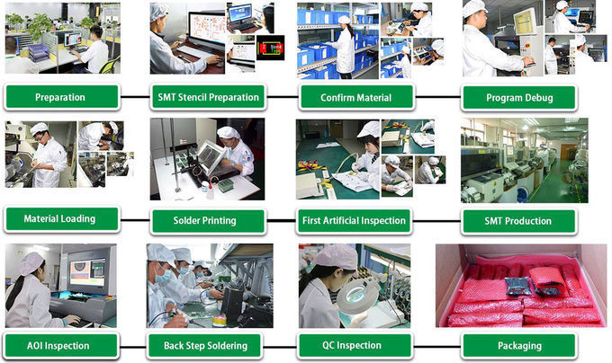
PCB, FPC process production capability
Product Details:
Place of Origin:China
Brand Name:XCE
Certification:CE,ROHS, FCC,ISO9008,SGS,UL
Model Number:XCEH
Minimum Order Quantity:1pcs
Price:negotiation
Packaging Details:inner: vacuum-packed bubble bag outer: carton box
Delivery Time:5-10 days
Payment Terms:T/T,Western union
Supply Ability:1, 000, 000 PCS / week
Advantage Highlights
Parameter:
| o | Item | Data |
| 1 | Layer: | 1 to 24 layers |
| 2 | Material type: | FR-4, CEM-1, CEM-3, High TG, FR4 Halogen Free, Rogers |
| 3 | Board thickness: | 0.20mm to 3.4mm |
| 4 | Copper thickness: | 0.5 OZ to 4 OZ |
| 5 | Copper thickness in hole: | >25.0 um (>1mil) |
| 6 | Max. Board Size: | (580mm×1200mm) |
| 7 | Min. Drilled Hole Size: | 4mil(0.1mm) |
| 8 | Min. Line Width: | 3mil (0.075mm) |
| 9 | Min. Line Spacing: | 3mil (0.075mm) |
| 10 | Surface finishing: | HASL / HASL lead free, HAL, Chemical tin, Chemical Gold, Immersion Silver/Gold, OSP, Gold plating |
| 11 | Solder Mask Color: | Green/Yellow/Black/White/Red/Blue |
| 12 | Shape tolerance: | ±0.13 |
| 13 | Hole tolerance: | PTH: ±0.076 NPTH: ±0.05 |
| 14 | Package: | Inner packing: Vacuum packing / Plastic bag,Outer packing: Standard carton packing |
| 15 | Certificate: | UL,SGS,ISO 9001:2008 |
| 16 | Special requirements: | Buried and blind vias+controlled impedance +BGA |
| 17 | Profiling: | Punching, Routing, V-CUT, Beveling |
Place of Origin: | Guangdong China (Mainland) | Brand Name: | XCE | Model Number: | XCEPCB008 |
Base Material: | FR4 | Copper Thickness: | 0.3-3oz | Board Thickness: | 0.3-6mm |
Min. Hole Size: | 0.2mm | Min. Line Width: | 3mil | Min. Line Spacing: | 3mil |
Surface Finishing: | HASL, OSP, Immersion Gold/Au, Immersion silver, etc. | Solder mask: | Green | PCB Standard: | IPC-A-610 E Class II-III |
Wrap and twist: | 5% | Layer Count: | 1-22 | profiling punching: | Routing, V-CUT, Beveling |
Max board size: | 1200mm*600mm | Hole tolerance: | PTH:±0.075,NTPH:±0.05 | PCB Tolerance of finished thickness: | ±5% |
PCB: | Customized | Product name: | pcb |
Benefits:
High dielectric constant for circuit size reduction
Low loss. Ideal for operating at X-band or below
Tight εr and thickness control for repeatable circuit performance
Typical Applications:
Space Saving Circuitry
Patch Antennas
Satellite Communications Systems
Power Amplifiers
Aircraft Collision Avoidance Systems
Ground Radar Warning Systems
Competitive Advantage:
1) With UL,ROHS,ISO,IPC
2).Lead time:3-10 working days
3)Competitive price best quality
4)Rich 20 years experience in High Tg Multilayer PCB
| Items | Manufacturing Capabilities | Remarks | |
|---|---|---|---|
| Number of Layers | – | 1-10 layers | For orders above 10 layers,please view the below “Standard PCB” or contact our sales rep. |
| Material | – | FR-4,Aluminum | For Flex, Rigid-flex, Metal-based (Aluminum etc.,), HDI, Halogen-free, High Tg, etc.,please view the below “Standard PCB” or contact sales rep. |
| Maximum PCB Size(Dimension) | – | 500*1100mm (min 5*6mm) | Any sizes beyond this dimension, please view the below “Standard PCB” or contact sales rep. |
| Board Size Tolerance(Outline) | – | ±0.2mm/±0.5mm | ±0.2mm for CNC routing, and ±0.5mm for V-scoring. |
| Board Thickness | 0.2-2.4mm | 0.2,0.4, 0.6, 0.8, 1.0, 1.2, 1.6, 2.0, 2.4mm. Please view the below “Standard PCB” or contact us if your board exceeds these. | |
| Board Thickness Tolerance(t≥1.0mm) | – | ±10% | Normally “+ Tolerance” will occur due to PCB processing steps such as electroless copper, solder mask and other types of finish on the surface. |
| Board Thickness Tolerance(t<1.0mm) | – | ±0.1mm | |
| Min Trace | 0.1mm/4mil | Min manufacturable trace is 4mil(0.1mm), strongly suggest to design trace above 6mil(0.15mm) to save cost. | |
| Min Spacing | Min manufacturable spacing is 4mil(0.1mm), strongly suggest to design spacing above 6mil(0.15mm) to save cost. | ||
| Outer Layer Copper Thickness | 1oz/2oz/3oz(35μm/70μm/105μm) | Also known as copper weight. 35μm=1oz, 70μm=2oz, 105μm=3oz. Please view the below “Standard PCB” or contact us if you need copper weight greater than 3oz. | |
| Inner Layer Copper Thickness | 1oz/1.5oz(35μm/50μm) | Inner copper weight as per customer’s request for 4 and 6 layers. Please contact us if you need copper weight greater than 1.5oz. | |
| Drill Sizes (CNC) | 0.2-6.3mm | Min drill size is 0.2mm, max drill is 6.3mm. Any holes greater than 6.3mm or smaller than 0.3mm will be subject to extra charges. | |
| Min Width of Annular Ring | 0.15mm(6mil) | For pads with vias in the middle, Min width for Annular Ring is 0.15mm(6mil). | |
| Finished Hole Diameter (CNC) | 0.2mm-6.2mm | The finished hole diameter will be smaller than size of drill bits because of copper plating in the hole barrels | |
| Finished Hole Size Tolerance(CNC) | – | ±0.08mm | For example, if the drill size is 0.6mm, the finished hole diameter ranges from 0.52mm to 0.68mm will be considered acceptable. |
| Solder Mask | LPI | Liquid Photo-Imageable is the mostly adopted. Thermosetting Ink is used in the inexpensive paper-based boards. | |
| Minimum Character Width(Legend) | 0.15mm | Characters of less than 0.15mm wide will be too narrow to be identifiable. | |
| Minimum Character Height (Legend) | – | 0.8mm | Characters of less than 0.8mm high will be too small to be recognizable. |
| Character Width to Height Ratio (Legend) | – | 1:5 | In PCB silkscreen legends processing, 1:5 is the most suitable ratio |
| Minimum Diameter of Plated Half Holes | – | 0.6mm | Design Half-Holes greater than 0.6mm to ensure better connection between boards. |
| Surface Finishing | HASL with lead HASL lead free Immersion gold,OSP | The most popular three types of PCB surface finish. Please view the below “Standard PCB” or contact us for other finishes. | |
| Solder Mask | Green ,Red, Yellow, Blue, White ,Black | No extra charge (Green, Red, Yellow, Blue) | |
| Silkscreen | White, Black, None | No extra charge. | |
| Panelization | V-scoring, Tab-routing, Tab-routing with Perforation (Stamp Holes) | Leave min clearance of 1.6mm between boards for break-routing. For V-score panelization, set the space between boards to be zero. | |
| Others | – | Fly Probe Testing (Free) and A.O.I. testing(free), ISO 9001:2008 ,UL Certificate | No extra charge. |
| Items | Sample | High Volume |
| Single Sided PCB | 1-3 | 4-7 |
| Double Sided PCB | 2-5 | 7-10 |
| Multi-layer PCB | 7-8 | 10-15 |
| PCB Making & Assembly | 8-15 | 15-20 |