Active Member
|
[China]

Address: Huishang Building, 19-128 Nathan Road, Yau Tsim Sha Tsui, Yau Tsim, Hong Kong
Contact name:Mank.Li

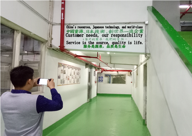
Shenzhen Chaosheng Electronic Technology Co.,Ltd |
|
|
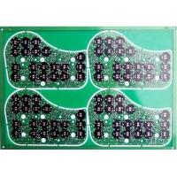
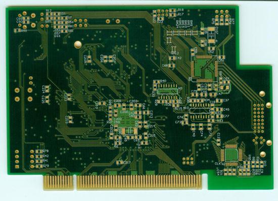
8-layer carbon oil + FR4 TG 150, type PCB, printed circuit board pcb multilayer pcb board Contact PCB PCBway-The PCB
8 layer FR4 Multilayer PCB with ENIG surface finish,1.6mm board thickness with 2.0oz copper thickness for communication products.
| PRODUCT’S DETAILS | |
| Raw Material | FR-4 (Tg 180 available) |
| Layer Count | 8-Layer |
| Board Thickness | 1.6mm |
| Copper Thickness | 2.0oz |
| Surface Finish | ENIG(Electroless Nickel Immersion Gold) |
| Solder Mask | Green |
| Silkscreen | White |
| Min. Trace Width/Spacing | 0.075/0.075mm |
| Min. Hole Size | 0.25mm |
| Hole Wall Copper Thickness | ≥20μm |
| Measurement | 300×400mm |
| Packaging | Inner: Vacuum-packed in soft plastic bales Outer: Cardboard Cartons with double straps |
| Application | Communication,automobile,cell,computer,medical |
| Advantage | Competitive Price,Fast Delivery,OEM&ODM,Free Samples, |
| Special Requirements | Buried And Blind Via, Impedance Control, Via Plug, BGA Soldering And Gold Finger Are Acceptable |
| Certification | UL,ISO9001:2008,ROHS,REACH,SGS,HALOGEN-FREE |
| PRODUCTION CAPABILITY OF PCB | ||
| Process Engineering | Items | Manufacturing Capability |
| Laminate | Thickness | 0.2~3.2mm |
| Production Type | Layer Count | 2L-16L |
| Cut Lamination | Max. Working Panel size | 1000×1200mm |
| Inner Layer | Internal Core Thickness | 0.1~2.0mm |
| Internal width/spacing | Min: 4/4mil | |
| Internal Copper Thickness | 1.0~3.0oz | |
| Dimension | Board Thickness Tolerance | ±10% |
| Interlayer Alignment | ±3mil | |
| Drilling | Manufacture Panel Size | Max: 650×560mm |
| Drilling Diameter | ≧0.25mm | |
| Hole Diameter Tolerance | ±0.05mm | |
| Hole Position Tolerance | ±0.076mm | |
| Min.Annular Ring | 0.05mm | |
| PTH+Panel Plating | Hole Wall copper Thickness | ≧20um |
| Uniformity | ≧90% | |
| Outer Layer | Track Width | Min: 0.08mm |
| Track Spacing | Min: 0.08mm | |
| Pattern Plating | Finished Copper Thickness | 1oz~3oz |
| EING/Flash Gold | Nickel Thickness | 2.5um~5.0um |
| Gold Thickness | 0.03~0.05um | |
| Solder Mask | Thickness | 15~35um |
| Solder Mask Bridge | 3mil | |
| Legend | Line width/Line spacing | 6/6mil |
| Gold Finger | Nickel Thickness | ≧120u〞 |
| Gold Thickness | 1~50u〞 | |
| Hot Air Level | Tin Thickness | 100~300u〞 |
| Routing | Tolerance of Dimension | ±0.1mm |
| Slot Size | Min:0.4mm | |
| Cutter Diameter | 0.8~2.4mm | |
| Punching | Outline Tolerance | ±0.1mm |
| Slot Size | Min:0.5mm | |
| V-CUT | V-CUT Dimension | Min:60mm |
| Angle | 15°30°45° | |
| Remain Thickness Tolerance | ±0.1mm | |
| Beveling | Beveling Dimension | 30~300mm |
| Test | Testing Voltage | 250V |
| Max.Dimension | 540×400mm | |
| Impedance Control | Tolerance | ±10% |
| Aspect Ration | 12:1 | |
| Laser Drilling Size | 4mil(0.1mm) | |
 |
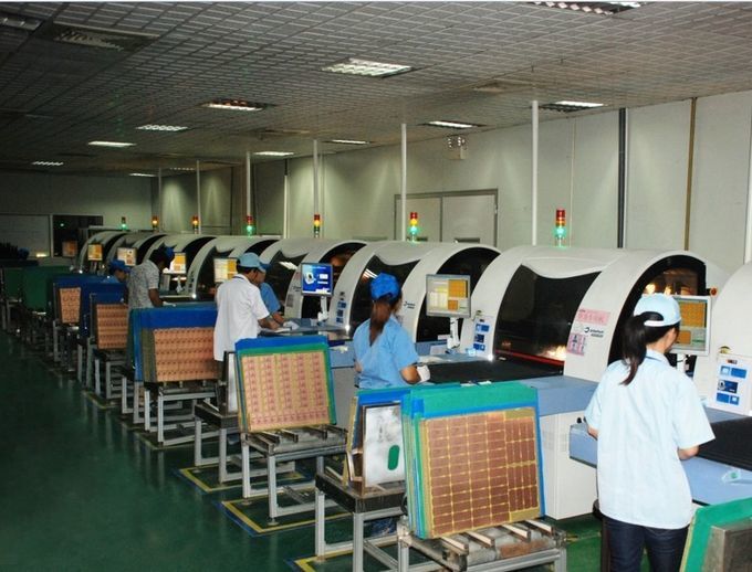
PCB, FPC process production capability
1: Medical Bluetooth module motherboard
2: Halogen-free FR-4 TG180, inner and outer copper thickness 35um, minimum line width line spacing 3/3mil, hole ratio 10:1, minimum hole 0.10mm, blind hole buried hole, immersion gold, red solder resist, white
3: The board thickness is 1.60mm,
4: blind hole, resin plug hole + plating hole
Printed Circuit Boards are 94V0 compliant, and adhere to IPC610 Class 2 international PCB
Standard.
Quantities range from prototype to volume production.
100% E-Test
PCB, FPC process production capability
| Technical ltem | MassProduct | Advanced Technology | |||||
| 2016 | 2017 | 2018 | |||||
| Max.Layer Count | 26L | 36L | 80L | ||||
| Through-hole plate | 2~45L | 2~60L | 2~80L | ||||
| Max.PCBSize(in) | 24*52" | 25*62" | 25*78.75" | ||||
| The layer number of FPC | 1~36L | 1~50L | 1~60L | ||||
| Max.PCBSize(in) | 9.8"*196" | 9.8"*196" | 10"*196"Reel to reel | ||||
| Layeredplatelayer | 2~12L | 2~18L | 2~26L | ||||
| Max.PCBSize(in) | 9"*48" | 9"*52" | 9"*62" | ||||
| Combination of hard and soft layers | 3~26L | 3~30L | 3~50L | ||||
| Interconnect HDI | 5+X+5Interconnect HDI | 7+X+7Interconnect HDI | 8+X+8,Interconnect HDI | ||||
| HDI PCB | 4~45L | 4~60L | 4~80L | ||||
| Interconnect HDI | 3+20+3 | 4+X+4Interconnect HDI | 4+X+4,Interconnect HDI | ||||
| Max.PCBSize(in) | 24"*43" | 24"*49" | 25"*52" | ||||
| Material | FR-4 Rogers | FR-4 Rogers | FR-4 Rogers | ||||
| Base material | Halogenfree,LowDK | Halogenfree,LowDK | Halogenfree,LowDK | ||||
| Build-up Material | FR-4 | FR-4 | FR-4 | ||||
| BOard,Thickness(mm) | Min.12L(mm) | 0.43 | 0.42~8.0mm | 0.38~10.0mm | |||
| Min.16L(mm) | 0.53 | 1.60~8.0mm | 0.45~10.0mm | ||||
| Min.18L(mm) | 0.63 | 2.0~8.0 | 0.51~10.0mm | ||||
| Min.52L(mm) | 0.8 | 2.50~8.0mm | 0.65~10.0mm | ||||
| MAX(mm) | 3.5 | 10.0mm | 10.0mm | ||||
| Min.CoreThickness um(mil) | 254"(10.0) | 254"(10.0) | 0.10~254(10.0mm) | ||||
| Min.Build up Dielectric | 38(1.5) | 32(1.3) | 25(1.0) | ||||
| BaseCopperWeight | Inner Layer | 4/1-8 OZ | 4/1-15 OZ | 4/1-0.30mm | |||
| Out Layer | 4/1-10 OZ | 4/1-15 OZ | 4/1-30 OZ | ||||
| Gold thick | 1~40u" | 1~60u" | 1~120u" | ||||
| Nithick | 76~127u" | 76~200u" | 1~250u" | ||||
| Min.HOle/Land um(mil) | 150/300(6/12) | 100/200(4/8) | 100/200(4/8) | ||||
| Min.Laser via/landum(mil) | 60/170(2.4/6.8) | 50/150(2/6) | 50/150(2/6) | ||||
| Min. IVH,Hole size/landum(mil) | 150/300(6/12) | 100/200(4/8) | 100/200(4/8) | ||||
| DieletricThickness | 38(1.5) | 32(1.3) | 32(1.3) | ||||
| 125(5) | 125(5) | 125(5) | |||||
| SKipvia | Yes | Yes | Yes | ||||
| viaoNhie(laserviaon BuriedPTH) | Yes | Yes | Yes | ||||
| Laser Hole Filling | Yes | Yes | Yes | ||||
| Technicalltem | Mass Product | Advanced Technolgy | |||||
| 2017year | 2018year | 2019year | |||||
| Drill hole depth ratio | ThroughHole | 2017year | .40:1 | .40:1 | |||
| Aspet Ratio | Micro Via | .35:1 | 1.2:1 | 1.2:1 | |||
| Copper Filling Dimple Size um(Mil) | 10(0.4) | 10(0.4) | 10(0.4) | ||||
| Min.LineWidth&space | lnner Layer um(mil) | 45/45(1.8/1.8) | 38/38(1.5/1.5) | 38/38(1.5/1.5) | |||
| Plated Layer um(mil) | 45/45(1.8/1.8) | 38/38(1.5/1.5) | 38/38(1.5/1.5) | ||||
| BGAPitch mm(Mil) | 0.3 | 0.3 | 0.3 | ||||
| Min.PTH Hole ring um(mil) | 75(3mil) | 62.5(2.5mil) | 62.5(2.5mil) | ||||
| Line Width Control | ∠2.5MIL | ±0.50 | ±0.50 | ±0.50 | |||
| 2.5Mil≤L/W∠4mil | ±0.50 | ±0.50 | ±0.50 | ||||
| ≦3mil | ±0.60 | ±0.60 | ±0.60 | ||||
| Laminated structure | Layer by layer | 3+N+3 | 4+N+4 | 5+N+5 | |||
| Sequential Build-up | 20L Any Layer | 36L Any Layer | 52L Any Layer | ||||
| Multi-layer overlay | N+N | N+N | N+N | ||||
| N+X+N | N+X+N | N+X+N | |||||
| sequential Lamination | 2+(N+X+N)+2 | 2+(N+X+N)+2 | 2+(N+X+N)+2 | ||||
| Soft and hard bonding | 2+(N+X+N)+2 | 2+(N+X+N)+2 | 2+(N+X+N)+2 | ||||
| PTH filling process | PTH resin plug hole + plating fill Electroplated hole/copper plug hole | PTH resin plug hole + plating fill Electroplated hole/copper plug hole | PTH resin plug hole + plating fill Electroplated hole/copper plug hole | ||||