Active Member
|
[China]

Address: Huishang Building, 19-128 Nathan Road, Yau Tsim Sha Tsui, Yau Tsim, Hong Kong
Contact name:Mank.Li

Shenzhen Chaosheng Electronic Technology Co.,Ltd |
|
|
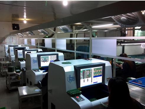
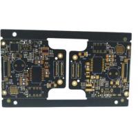
We are reliable and competitive manufacturer of PCBs with advanced technology,experienced workers,professional salesteam and competitive prices and high quality,we mainly specialize in 1 layer,2 layers,4 layers to 10 layers,60 layersHDI,we offer HAL,OSP,immersion gold,etc,no MOQ , rosh compliant, all we need is your gerber file and quantity,then we will quote best price and do best for you,it is very easy,welcome to inquire anytime, tks for your interest.
Process parameters:
| Content | Capability |
| Material | FR4, TG130, TG140, TG160, TG170 TG180 TG240 |
| Surface treatment | HASL,Chemical Tin,ENIG(Immersion GOLD),OSP,IMT,Plating silver,GOLD Finger |
| Layers | Single-sided,double-sided,4 layers, 6,8,10,20 30 40 60 Layers |
| Maxi. board size | 800mmX508mm |
| Line width/space | 0.1mm/ 0.1mm |
| Board thickness | 0.2mm-4mm |
| Min.tolerance of Board thickness | +/-8% - 10% |
| Copper foil thickness | Out Layer:17.5um/35um/70um/105um/140um/175um Inner Layer:17.5um/35um/70um/105um/140um |
| Outline Tolerance | CNC routing:+/-0.1mm , Punching: +/-0.1mm |
| V-CUT registration | +/-0.15mm |
| PTH hole copper thickness | 15um-50um |
| Warp and twist | <=1% |
| Min registration of hole position | +/-3mil(+/-0.76mm) |
| Min punching hole | 0.8mm(Board thickness below 1.0mm .) |
| Min Punching Square slot | (Board thickness below 1.0mm, 1.0mmX1.0mm) |
| Registration of printed circuit | +/-0.076mm |
| Min drill hole diameter | 0.2mm |
| Min tolerance of hole diameter | +/-0.05mm |
| Thickness of surface treatment | Plating Gold:(Ni4um-6um ,Au 0.1um-0.5um) Immersion GOLD: (Ni 5um-6um,Au:0.0254um-0.127um) Plating Silver:(Ag 5um-8um) |
| V-CUT degree tolerance | +/-5(degree) |
| V-CUT Board thickness | 0.6mm-3.2mm |
| Min Legend width | 0.1mm |
| Min Solder mask width | 0.1mm |
| Min Solder mask ring | 0.05mm |
PCB, FPC process production capability
| Technical ltem | MassProduct | Advanced Technology | |||||
| 2016 | 2017 | 2018 | |||||
| Max.Layer Count | 26L | 36L | 80L | ||||
| Through-hole plate | 2~45L | 2~60L | 2~80L | ||||
| Max.PCBSize(in) | 24*52" | 25*62" | 25*78.75" | ||||
| The layer number of FPC | 1~36L | 1~50L | 1~60L | ||||
| Max.PCBSize(in) | 9.8"*196" | 9.8"*196" | 10"*196"Reel to reel | ||||
| Layeredplatelayer | 2~12L | 2~18L | 2~26L | ||||
| Max.PCBSize(in) | 9"*48" | 9"*52" | 9"*62" | ||||
| Combination of hard and soft layers | 3~26L | 3~30L | 3~50L | ||||
| Interconnect HDI | 5+X+5Interconnect HDI | 7+X+7Interconnect HDI | 8+X+8,Interconnect HDI | ||||
| HDI PCB | 4~45L | 4~60L | 4~80L | ||||
| Interconnect HDI | 3+20+3 | 4+X+4Interconnect HDI | 4+X+4,Interconnect HDI | ||||
| Max.PCBSize(in) | 24"*43" | 24"*49" | 25"*52" | ||||
| Material | FR-4 Rogers | FR-4 Rogers | FR-4 Rogers | ||||
| Base material | Halogenfree,LowDK | Halogenfree,LowDK | Halogenfree,LowDK | ||||
| Build-up Material | FR-4 | FR-4 | FR-4 | ||||
| BOard,Thickness(mm) | Min.12L(mm) | 0.43 | 0.42~8.0mm | 0.38~10.0mm | |||
| Min.16L(mm) | 0.53 | 1.60~8.0mm | 0.45~10.0mm | ||||
| Min.18L(mm) | 0.63 | 2.0~8.0 | 0.51~10.0mm | ||||
| Min.52L(mm) | 0.8 | 2.50~8.0mm | 0.65~10.0mm | ||||
| MAX(mm) | 3.5 | 10.0mm | 10.0mm | ||||
| Min.CoreThickness um(mil) | 254"(10.0) | 254"(10.0) | 0.10~254(10.0mm) | ||||
| Min.Build up Dielectric | 38(1.5) | 32(1.3) | 25(1.0) | ||||
| BaseCopperWeight | Inner Layer | 4/1-8 OZ | 4/1-15 OZ | 4/1-0.30mm | |||
| Out Layer | 4/1-10 OZ | 4/1-15 OZ | 4/1-30 OZ | ||||
| Gold thick | 1~40u" | 1~60u" | 1~120u" | ||||
| Nithick | 76~127u" | 76~200u" | 1~250u" | ||||
| Min.HOle/Land um(mil) | 150/300(6/12) | 100/200(4/8) | 100/200(4/8) | ||||
| Min.Laser via/landum(mil) | 60/170(2.4/6.8) | 50/150(2/6) | 50/150(2/6) | ||||
| Min. IVH,Hole size/landum(mil) | 150/300(6/12) | 100/200(4/8) | 100/200(4/8) | ||||
| DieletricThickness | 38(1.5) | 32(1.3) | 32(1.3) | ||||
| 125(5) | 125(5) | 125(5) | |||||
| SKipvia | Yes | Yes | Yes | ||||
| viaoNhie(laserviaon BuriedPTH) | Yes | Yes | Yes | ||||
| Laser Hole Filling | Yes | Yes | Yes | ||||
| Technicalltem | Mass Product | Advanced Technolgy | |||||
| 2017year | 2018year | 2019year | |||||
| Drill hole depth ratio | ThroughHole | 2017year | .40:1 | .40:1 | |||
| Aspet Ratio | Micro Via | .35:1 | 1.2:1 | 1.2:1 | |||
| Copper Filling Dimple Size um(Mil) | 10(0.4) | 10(0.4) | 10(0.4) | ||||
| Min.LineWidth&space | lnner Layer um(mil) | 45/45(1.8/1.8) | 38/38(1.5/1.5) | 38/38(1.5/1.5) | |||
| Plated Layer um(mil) | 45/45(1.8/1.8) | 38/38(1.5/1.5) | 38/38(1.5/1.5) | ||||
| BGAPitch mm(Mil) | 0.3 | 0.3 | 0.3 | ||||
| Min.PTH Hole ring um(mil) | 75(3mil) | 62.5(2.5mil) | 62.5(2.5mil) | ||||
| Line Width Control | ∠2.5MIL | ±0.50 | ±0.50 | ±0.50 | |||
| 2.5Mil≤L/W∠4mil | ±0.50 | ±0.50 | ±0.50 | ||||
| ≦3mil | ±0.60 | ±0.60 | ±0.60 | ||||
| Laminated structure | Layer by layer | 3+N+3 | 4+N+4 | 5+N+5 | |||
| Sequential Build-up | 20L Any Layer | 36L Any Layer | 52L Any Layer | ||||
| Multi-layer overlay | N+N | N+N | N+N | ||||
| N+X+N | N+X+N | N+X+N | |||||
| sequential Lamination | 2+(N+X+N)+2 | 2+(N+X+N)+2 | 2+(N+X+N)+2 | ||||
| Soft and hard bonding | 2+(N+X+N)+2 | 2+(N+X+N)+2 | 2+(N+X+N)+2 | ||||
| PTH filling process | PTH resin plug hole + plating fill Electroplated hole/copper plug hole | PTH resin plug hole + plating fill Electroplated hole/copper plug hole | PTH resin plug hole + plating fill Electroplated hole/copper plug hole | ||||
PCB, FPC main material supplier
| NO | supplier | Supply material name | Material origin | |||||
| 1 | Japan | High frequency materials, PI, covering membrane,Copper berth | Mitsubishi Japan | |||||
| 2 | dupont | High frequency materials, PI, covering film, dry film,Copper berth | Japan | |||||
| 3 | panasonic | High frequency materials, PI, covering membrane,Copper berth | Japan | |||||
| 4 | SanTie | PI, covering membrane | Japan | |||||
| 5 | Born good | FR-4,PI,PP,Copper berth | shenzhen, China | |||||
| 6 | A rainbow | PI, covering membrane,Copper berth | Taiwan | |||||
| 7 | teflon | High frequency materials | The United States | |||||
| 8 | Rogers | High frequency materials | The United States | |||||
| 9 | Nippon Steel | PI, covering membrane,Copper berth | Taiwan | |||||
| 10 | sanyo | PI, covering membrane,Copper berth | Japan | |||||
| 11 | South Asia | FR-4,PI,PP,Copper berth | Taiwan | |||||
| 12 | doosan | FR-4,PP | South Korea | |||||
| 13 | Tai Yao plate | FR-4,PP,Copper berth | Taiwan | |||||
| 14 | Alight | FR-4,PP,Copper berth | Taiwan | |||||
| 15 | Yaoguang | FR-4,PP,Copper berth | Taiwan | |||||
| 16 | Yalong | FR-4,PP | The United States | |||||
| 17 | ISOAL | FR-4,PP | Japan | |||||
| 18 | OAK | Buried, buried resistance, PP | Japan | |||||
| 19 | United States 3M | FR-4,PP | The United States | |||||
| 20 | Bergs | Copper and aluminum matrix | Japan | |||||
| 21 | The sun | ink | Taiwan | |||||
| 22 | Murata | ink | Japan | |||||
| 23 | generous andbenevolent | PI, covering membrane,Copper berth | China's jiangxi | |||||
| 24 | Yasen | PPI, covering membrane | China jiangsu | |||||
| 25 | Yong Sheng Tai | ink | China guangdong panyu | |||||
| 26 | mita | ink | Japan | |||||
| 27 | Transcript | ceramic material | Taiwan | |||||
| 28 | HOME | ceramic material | Japan | |||||
| 29 | Fe-Ni-Mn | Alloy Invar, Section Steel | Taiwan | |||||