
|
|
[China]

Trade Verify
Address: Building C5/B6, Yanchuan North Industrial Park, Yanluo Street, Baoan District, Shenzhen, China
Contact name:Rachel

Shenzhen Benqiang Circuits Co,Ltd. |
|
Verified Suppliers
|
|
|
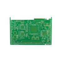
High-Density Multilayer PCB with 6-Layer Design for High Density Interconnector
The HDI PCB Board, also known as High-Density Interconnector PCB, is a cutting-edge product designed for the most advanced electronic devices. With its unique design and advanced features, this PCB board is the perfect solution for high-density circuitry and complex electronic systems.
The HDI PCB Board is a high-density layered PCB that is specifically designed for high-performance electronic devices. It allows for a higher number of connections and more complex circuitry in a smaller and more compact space, making it ideal for advanced electronics such as smartphones, tablets, and other portable devices.
This PCB board is designed to meet the growing demand for smaller, faster, and more powerful electronic devices. With its advanced features and technologies, it enables the design and production of complex nanocircuit boards, making it a highly sought-after product in the electronics industry.
The HDI PCB Board is widely used in various electronic devices such as smartphones, tablets, laptops, GPS devices, and other portable electronics. It is also used in advanced medical equipment, aerospace technology, and military and defense systems.
Due to its advanced features and capabilities, the HDI PCB Board is an essential component in the development of high-performance electronic devices. Its high-density layered design and nanocircuit capabilities make it the preferred choice for designers and manufacturers in the electronics industry.
The HDI PCB Board is a revolutionary product that is changing the landscape of advanced electronics. With its high-density layered design, nanocircuit capabilities, and advanced features, it enables the production of smaller, faster, and more powerful electronic devices. Its superior performance, reliability, and durability make it the go-to solution for high-performance electronics. Choose the HDI PCB Board for your next project and experience the future of advanced electronics.
| Parameter | Description |
|---|---|
| Stencil Service | Yes |
| Pcb Name | 4L 1+N+1 HDI Boards |
| Board Size | 300 * 210 Mm |
| Pcb Thickness | 1.5 Mm |
| Number Of Layers | 6-Layer |
| Pcb Test | 100% Testing |
| Surface Finishing | Chemical Nickel Palladium |
| Layer Count | 1-30 Layers |
| Glass Epoxy | RO4350B Tg280℃, Er<3.48, Rogers Corp |
| Impedance Control | Yes |
| Microvia Technology Board | HDI (High-Density Interconnect) technology is used to create microvias, allowing for higher density of traces and smaller PCBs. |
| Advanced Interconnect PCB | HDI PCBs use advanced interconnect technologies to increase the number of connections and reduce signal loss, making them suitable for high-speed and high-frequency applications. |
| High-Density Multilayer PCB | This PCB has a high density of components and layers, making it suitable for compact and complex electronic designs. |
HDI PCB Board, also known as High-Density Interconnect PCB, is a cutting-edge technology that has revolutionized the world of electronics. With the increasing demand for smaller, faster, and more reliable devices, HDI PCB has emerged as a game-changer in the field of electronic design and manufacturing.
HDI PCB Board is mainly used as a main board in electronic devices due to its high-speed performance and advanced design capabilities. It can be found in a wide range of products, such as smartphones, laptops, tablets, and other electronic devices.
One of the key features of HDI PCB Board is its ability to incorporate complex designs and high-density interconnects. This is made possible by the use of a stencil, which is a thin sheet of metal with cutouts that allow for precise placement of components on the PCB. With the help of stencil service, HDI PCBs can be manufactured with high precision and accuracy, ensuring optimal performance.
HDI PCB Board is made using high-quality glass epoxy material, specifically RO4350B Tg280℃ with a dielectric constant (Er) of less than 3.48, provided by Rogers Corp. This material offers excellent thermal stability, high mechanical strength, and low dielectric loss, making it suitable for high-frequency applications.
HDI PCB Board is manufactured with a thickness of 1.5mm, making it thinner and more compact compared to traditional PCBs. This allows for more efficient use of space and enables the miniaturization of electronic devices, meeting the demand for smaller and sleeker products.
As the name suggests, HDI PCB Board is known for its high-density interconnect capabilities. It allows for the placement of a large number of components in a small area, resulting in a high-density layered PCB. This not only reduces the overall size of the PCB but also improves its performance by reducing signal loss and improving signal integrity.
With its advanced design and manufacturing capabilities, HDI PCB Board is suitable for a wide range of applications. Some of the common scenarios where HDI PCB Board is used include:
In conclusion, HDI PCB Board has become an essential component in the world of electronics, enabling the development of smaller, faster, and more reliable devices. Its high-density interconnect technology and advanced design capabilities make it a preferred choice for various applications, providing high-speed performance and high reliability in a small form factor.
Product Description: Our HDI PCB Board is a high-density multilayer PCB that utilizes advanced PCB technology to create a nanocircuit PCB. This allows for smaller and more complex designs, making it ideal for high-tech electronic devices.
Features:
Customization Options:
Why Choose Our HDI Interconnect Board Customization Service?
Get in touch with us today to learn more about our HDI Interconnect Board Customization Service and how we can help bring your high-tech electronic devices to life.
For the packaging and shipping of our HDI PCB Boards, we take great care to ensure that your order arrives safely and in pristine condition. Our packaging process follows industry standards and is tailored to meet the specific requirements of HDI PCB boards.
Firstly, the HDI PCB boards are carefully inspected and cleaned to remove any dust or debris. They are then wrapped in anti-static material to protect against electrostatic discharge (ESD).
Next, the boards are placed in a sturdy, custom-fit box that provides cushioning and protection during shipping. The box is sealed with tape and labeled with the necessary information, including the customer's name, address, and order details.
In some cases, depending on the size and fragility of the order, additional packaging materials such as bubble wrap or foam inserts may be used to further protect the HDI PCB boards during transit.
We offer a variety of shipping options to suit your needs and budget. Our standard shipping method is through a trusted courier service, which provides tracking information and ensures a timely delivery.
For urgent orders, we also offer expedited shipping options such as express delivery or air freight. Please contact us for more details and pricing.
We ship our HDI PCB boards worldwide to meet the needs of our global customers. We carefully follow all international shipping regulations and ensure that all necessary customs documentation is completed accurately and on time.
For international orders, shipping times may vary depending on the destination country and any potential customs delays. Our team will provide you with an estimated delivery date and tracking information once your order has been shipped.
Thank you for choosing our HDI PCB boards. We are committed to delivering high-quality products and exceptional customer service, including our packaging and shipping process. If you have any questions or concerns, please do not hesitate to contact us.


