
|
|
[China]

Trade Verify
Address: Building C5/B6, Yanchuan North Industrial Park, Yanluo Street, Baoan District, Shenzhen, China
Contact name:Rachel

Shenzhen Benqiang Circuits Co,Ltd. |
|
Verified Suppliers
|
|
|
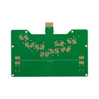
1-30 Layers HDI Printed Wiring Board with 100% Testing and Custom Solutions
HDI PCB Board, also known as High-Density Interconnect PCB Board, is a type of advanced printed circuit board that is widely used in the consumer electronics industry. With the ever-increasing demand for smaller and more powerful electronic devices, HDI PCB Boards have become the go-to solution for manufacturers looking to meet these requirements.
One of the key features of HDI PCB Boards is their use of Microvia Technology, which allows for the creation of densely packed circuits on a smaller board. This technology allows for the connection of multiple layers of circuitry without the need for through-hole vias, resulting in a more compact and efficient board design.
The HDI PCB Board is a high-density multilayer PCB, typically consisting of 4 or more layers, with 1+N+1 layer structure. This means that the board has one layer of core material, followed by a layer of circuitry, then a layer of insulating material, and so on. This layer structure allows for a more efficient use of space and improved signal integrity.
One of the key selling points of the HDI PCB Board is its ability to achieve precise impedance control. With the use of advanced manufacturing processes, the PCB is designed to have a specific impedance value to ensure optimal signal transmission. This makes it suitable for high-speed and high-frequency applications, such as in consumer electronics.
The HDI PCB Board comes in a standard board size of 300 * 210 mm, making it suitable for a wide range of consumer electronic devices. The board size can also be customized to meet specific design requirements, providing flexibility for manufacturers.
Another advantage of the HDI PCB Board is its range of silkscreen colors. Customers can choose from a variety of options, including white, black, yellow, red, blue, and more. This allows for easy identification and labeling of components on the board, making it easier for assembly and troubleshooting.
In conclusion, the HDI PCB Board is a highly advanced and versatile product that is ideal for use in consumer electronics. With its microvia technology, high-density multilayer design, precise impedance control, and customizable options, it offers an efficient and reliable solution for manufacturers looking to stay ahead in the constantly evolving electronics industry.
| Parameter | Value |
|---|---|
| Product Name | HDI PCB Board |
| Process | Immersion Gold |
| Number of Layers | 6-Layer |
| Layer Count | 1-30 Layers |
| PCB Thickness | 1.5 mm |
| Board Size | 300 * 210 mm |
| Application | Consumer Electronics |
| Impedance Control | Yes |
| Apply For | Main Board |
| Key Words | High Density Interconnector, High-Density Layered PCB, Microvia Technology Board, High-Density Multilayer PCB |
| Silkscreen Color | White, Black, Yellow, Red, Blue, etc. |
The HDI PCB Board, also known as the High Density Interconnect PCB Board, is an advanced interconnect PCB designed for high-performance and complex electronic devices. It is widely used in various industries such as telecommunications, automotive, aerospace, and medical equipment. The following is an introduction to the application scenarios of the HDI PCB Board.
The HDI PCB Board is coated with Chemical Nickel Palladium, a type of surface finishing that provides superior corrosion resistance, solderability, and durability. This ensures the reliability and longevity of the board, making it suitable for use in harsh environments.
The 4L 1+N+1 HDI Board is a type of HDI PCB Board with a unique structure of 4 layers, 1 layer of via-in-pad, and 1 layer of buried via. This design allows for a higher density of components on the board, making it ideal for use in compact electronic devices.
The HDI PCB Board is made of RO4350B Tg280℃, a high-performance glass epoxy material with a low dielectric constant (Er <3.48). This material, produced by Rogers Corporation, offers excellent electrical properties and thermal stability, making it suitable for high-speed and high-frequency applications.
The HDI PCB Board is commonly used as the main board in electronic devices. It serves as the central hub for all other components and plays a crucial role in the overall performance and functionality of the device.
The HDI PCB Board has 6 layers, which allows for a high level of integration and miniaturization of electronic circuits. This makes it a preferred choice for devices that require compact and lightweight designs.
The HDI PCB Board utilizes advanced interconnect technology, such as microvia and buried via, to achieve a higher density of components and interconnections. This results in improved signal integrity, reduced signal loss, and increased reliability of the board.
Microvia technology is a key feature of the HDI PCB Board. It involves the use of small diameter vias (less than 150 microns) to connect different layers of the board. This allows for a higher density of routing and smaller pad sizes, making it ideal for complex and high-speed circuit designs.
The HDI PCB Board is a highly versatile and advanced interconnect PCB that offers superior performance and reliability. With its unique features and capabilities, it is widely used in various industries and applications, making it an essential component in the modern electronic world.
Board Size: 300 * 210 Mm
Pcb Thickness: 1.5 Mm
Surface Finishing: Chemical Nickel Palladium
Layer Count: 1-30 Layers
Number Of Layers: 6-Layer
At our company, we specialize in providing high-quality customized services for HDI PCB Board. Our team of experts is dedicated to meeting your specific requirements and delivering top-notch solutions for your projects. With our advanced technology and state-of-the-art equipment, we are able to produce high-density PCB panels with up to 30 layers, making us a leader in the industry. Our high-density multilayer PCBs are designed to meet the demanding needs of various industries, including telecommunications, aerospace, medical, and more. We understand the importance of precision and reliability in these industries, and our HDI PCBs are manufactured to the highest standards to ensure optimal performance. One of our specialties is microvia PCB assembly, which allows for the miniaturization of electronic devices. With our advanced equipment and skilled technicians, we are able to create intricate and complex designs that are essential for today's advanced technology. We take great pride in our ability to produce high-density PCBs with microvias that are reliable and durable. In addition, our HDI PCB boards can be customized to your desired board size and thickness. With a board size of 300 * 210 mm and a thickness of 1.5 mm, we are able to accommodate a wide range of project needs. We also offer surface finishing options, such as chemical nickel palladium, to ensure the best performance and longevity of your HDI PCB boards. Choose our company for your high-density PCB needs and experience the difference of our top-quality customized services. Our team is committed to providing you with the best solutions and meeting your specific requirements. Contact us today to learn more about our HDI PCB board customization services.
At HDI PCB Board, we take great care in packaging and shipping our products to ensure their safe arrival at your doorstep. Here is a breakdown of our packaging and shipping process:
Rest assured, your HDI PCB Board will be packaged and shipped with the utmost care and attention to detail. If you have any specific packaging or shipping requests, please don't hesitate to let us know. We are always happy to accommodate our customers' needs.


