
|
|
[China]

Trade Verify
Address: Address:Room624,Fangdichan development building,Guicheng south,Nanhai,Foshan,China
Contact name:Tracy

ONESEINE TECHNOLOGY CO.,LTD |
|
Verified Suppliers
|
|
|
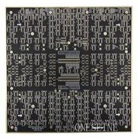
8Layer CEM-3 Material HDI High Density Interconnect Fr4 PCB Circuit Board
PCB parameter:
PCB material:CEM-3
Product name: automotive electronics pcb
Layer:8
Surface finish:ENIG
Copper weight:1OZ
Line width:6mil
Thickness:1.6mm
The difference between CEM-3 and FR-4
Double-sided and multi-layer printed circuit boards for electronic products now usually use FR-4 substrate, which is a copper-clad flame-retardant epoxy glass cloth board. CEM-3 is a new type of substrate material for printed circuit developed on the basis of FR-4. In recent years, Japan has adopted a large number of CEM-3 to replace FR-4, even exceeding the amount of FR-4. About 55% of double-sided panels use CEM-3. 1. CEM-3 is a composite copper clad laminate
FR-4 is made of copper foil and glass fiber cloth impregnated with flame retardant epoxy resin. The difference between CEM-3 and FR-4 is that it uses a composite substrate of glass cloth and glass mat, also known as composite Type substrate, not just glass cloth.
The production process of CEM-3 is similar to FR-4. The gluing of the glass mat can be vertical gluing or horizontal gluing. The epoxy resin system used is the same as FR-4. In order to improve performance, it can be modified, usually a certain amount of filler is added. The suppression pressure is generally half lower than FR-4. In order to meet the requirements of different thicknesses, glass mats of different standard weights can be used, and the commonly used ones are 50g, 75g, and 105g.
Second, CEM-3 performance
If CEM-3 wants to replace FR-4, it must achieve the various properties of FR-4. The current CEM-3 has overcome the defects of early CEM-3 products such as poor quality of punching metallization, warpage and dimensional stability by improving the resin system, glass mat, and lamination manufacturing process. CEM-3's glass transition temperature, immersion resistance, peeling strength, water absorption, electrical breakdown, insulation resistance, UL indicators, etc. can all meet the FR-4 standard, the difference is that CEM-3 has low bending strength
In FR-4, the thermal expansion is greater than FR-4.
CEM-3 metallized hole processing is not a problem, the drill bit wear rate of drilling processing is low, it is easy to punch and press forming processing, and the thickness and dimension accuracy are high, but the metalized appearance of punching is slightly worse. 3. CEM-3 market application
UL believes that CEM-3 and FR-4 are interchangeable, so the current double-sided FR-4 can generally be used as a replacement object. Because CEM-3 has similar performance to FR-4, it has become possible to substitute it on multilayer boards.
Due to the fierce price competition for printed circuit boards, the four-layer board market has also begun to consider CEM-3. But for thin plates (<0.8mm), the price advantage does not exist.
printed circuit boards made of CEM-3 are now used in fax machines, copiers, instruments, telephones, automotive electronics, household appliances and other products
How can I determine the characteristic impedance of transmission lines in my HDI PCB design?
1,Empirical Formulas: Empirical formulas provide approximate calculations of characteristic impedance based on simplified assumptions. The most commonly used formula is the microstrip transmission line formula, which is suitable for traces on an outer layer of the PCB. The formula is: Zc = (87 / √εr) * log(5.98h / W + 1.74b / W) Where:
Zc = Characteristic impedance
εr = Relative permittivity (dielectric constant) of the PCB material
h = Height of the dielectric material (trace thickness)
W = Width of the trace
b = Separation between the trace and the reference plane (ground plane) It is important to note that empirical formulas provide approximate results and may not account for all the complexities of the PCB structure.
2,Field Solver Simulations: To obtain more accurate results, electromagnetic field solver simulations can be performed using specialized software tools. These tools consider the specific layer stackup, trace geometry, dielectric materials, and other factors to accurately calculate the characteristic impedance. Field solver simulations take into account the effects of fringing fields, dielectric losses, and other factors that influence the impedance. Field solver software tools, such as Ansys HFSS, CST Studio Suite, or Sonnet, allow you to input the PCB structure, material properties, and trace dimensions to simulate the transmission line and obtain the characteristic impedance. These simulations provide more precise results and are recommended for high-frequency applications or when accurate impedance control is crucial.
HDI pcb application
HDI PCB technology finds applications in various industries and electronic devices where there is a need for high-density interconnects, miniaturization, and advanced circuitry. Some common applications of HDI PCBs include:
1,Mobile Devices: HDI PCBs are extensively used in smartphones, tablets, and other mobile devices. The compact size and high-density interconnects of HDI PCBs allow for the integration of multiple functionalities, such as processors, memory, sensors, and wireless communication modules, in a small form factor.,
2,Computing and Networking Equipment: HDI PCBs are employed in computing devices like laptops, ultrabooks, and servers, as well as networking equipment such as routers, switches, and data centers. These applications benefit from the high-density circuitry and optimized signal transmission capabilities of HDI PCBs to support high-speed data processing and network connectivity.
3,Medical Devices: HDI PCBs are used in medical equipment and devices, including diagnostic machines, imaging systems, patient monitoring systems, and implantable devices. The miniaturization achieved through HDI technology allows for smaller and more portable medical devices without compromising their functionality.,
4,Automotive Electronics: HDI PCBs are increasingly prevalent in automotive electronics due to the growing demand for advanced driver assistance systems (ADAS), infotainment systems, and vehicle connectivity. HDI PCBs enable the integration of complex electronics in a compact space, contributing to enhanced vehicle safety, entertainment, and communication capabilities.
5,Aerospace and Defense: HDI PCBs are utilized in aerospace and defense applications, including avionics systems, satellites, radar systems, and military communication equipment. The high-density interconnects and miniaturization offered by HDI technology are crucial for space-constrained environments and demanding performance requirements.,
6,Industrial and IoT Devices: HDI PCBs play a vital role in industrial automation, IoT (Internet of Things) devices, and smart devices used in home automation, energy management, and environmental monitoring. These applications benefit from the smaller size, improved signal integrity, and increased functionality provided by HDI PCBs.
What are some challenges in implementing HDI PCB technology in automotive electronics?
Implementing HDI PCB technology in automotive electronics does come with its set of challenges. Some of the key challenges include:
Reliability and Durability: Automotive electronics are subjected to harsh environmental conditions, including temperature variations, vibrations, and moisture. Ensuring the reliability and durability of HDI PCBs in such conditions becomes crucial. The materials used, including the substrates, laminates, and surface finishes, must be carefully selected to withstand these conditions and provide long-term reliability.
Signal Integrity: Automotive electronics often involve high-speed data transmission and sensitive analog signals. Maintaining signal integrity becomes challenging in HDI PCBs due to the increased density and miniaturization. Issues such as crosstalk, impedance matching, and signal degradation need to be carefully managed through proper design techniques, controlled impedance routing, and signal integrity analysis.
Thermal Management: Automotive electronics generate heat, and effective thermal management is essential for their reliable operation. HDI PCBs, with their higher circuit density, can have increased power densities, making heat dissipation more challenging. Proper thermal design considerations, including heat sinks, thermal vias, and effective cooling mechanisms, are necessary to prevent overheating and ensure the longevity of components.
Manufacturing Complexity: HDI PCBs involve more complex manufacturing processes compared to traditional PCBs. The sequential build-up process, laser drilling, and fine-pitch component assembly require specialized equipment and expertise. The challenges arise in maintaining tight manufacturing tolerances, ensuring accurate alignment of microvias, and achieving high yields during production.
Cost: The implementation of HDI PCB technology in automotive electronics can increase the overall manufacturing cost. The use of advanced materials, specialized manufacturing processes, and additional quality control measures can contribute to higher production expenses. Balancing the cost factor while meeting the performance and reliability requirements becomes a challenge for automotive OEMs.
Regulatory Compliance: Automotive electronics are subject to strict regulatory standards and certifications to ensure safety and reliability. Implementing HDI PCB technology while meeting these compliance requirements can be challenging, as it may involve additional testing, validation, and documentation processes.
Addressing these challenges requires collaboration between PCB designers, manufacturers, and automotive OEMs to develop robust design guidelines, select suitable materials, optimize manufacturing processes, and conduct thorough testing and validation. Overcoming these challenges is essential to leverage the benefits of HDI PCB technology in automotive electronics and deliver reliable and high-performance electronic systems in vehicles.


