
|
|
[China]

Trade Verify
Address: Address:Room624,Fangdichan development building,Guicheng south,Nanhai,Foshan,China
Contact name:Tracy

ONESEINE TECHNOLOGY CO.,LTD |
|
Verified Suppliers
|
|
|
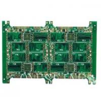
Buy China Circuit Board Fr5 Hdi PCB Manufacturing Process
PCB parameter:
Layer count:6
Meterials: FR-5
Thickness: 1.55MM
Copper foil thickness:35UM
Surface finish:ENIG 1U"
Min finish via dia:0.25mm
Min width/Sqacing:0.152MM/0.97MM
Are there any specific design rules or guidelines I should follow when determining the characteristic impedance in my HDI PCB design?
1,PCB Material Selection: The choice of dielectric material significantly influences the characteristic impedance. Select a PCB material with a known and consistent dielectric constant (relative permittivity) to achieve accurate impedance values. Consult with your PCB manufacturer for recommended materials suitable for high-frequency applications and impedance control.
2,Layer Stackup: The layer stackup configuration plays a crucial role in determining the characteristic impedance. Ensure consistent dielectric thickness between signal layers and maintain uniformity in the stackup across the PCB. Avoid abrupt changes in dielectric thickness or material in the signal path, as it can introduce impedance variations.
3,Trace Geometry: The width, spacing, and thickness of the traces impact the characteristic impedance. Follow the recommended trace width and spacing guidelines provided by your PCB manufacturer or use impedance calculators or simulation tools to determine the appropriate trace dimensions for the desired impedance value. Maintain consistent trace dimensions along the signal path to ensure impedance uniformity.
4,Differential Pairs: For differential signaling, maintain consistent trace widths, spacing, and length matching for the differential pairs. This helps in achieving balanced impedance and minimizing signal skew and common-mode noise.
5,Via Design: Vias can affect the characteristic impedance, especially in high-speed designs. Minimize the use of vias in the signal path, and if necessary, use controlled impedance vias (such as microvias) to maintain impedance continuity. Consider the impact of via stubs on impedance and minimize their length when possible.
6,Ground Plane Configuration: A solid and continuous ground plane beneath the signal traces helps in providing a low-inductance return path and reducing crosstalk and EMI. Ensure proper stitching vias or ground vias to connect the signal layers to the ground plane at regular intervals to maintain signal integrity.
7,Manufacturing Tolerances: Consider the manufacturing tolerances and capabilities of your PCB manufacturer when designing for impedance control. Consult their design guidelines for recommended tolerances for trace width, spacing, dielectric thickness, and layer stackup. These guidelines help ensure manufacturability while maintaining impedance accuracy.
HDI pcb application
HDI PCB technology finds applications in various industries and electronic devices where there is a need for high-density interconnects, miniaturization, and advanced circuitry. Some common applications of HDI PCBs include:
1,Mobile Devices: HDI PCBs are extensively used in smartphones, tablets, and other mobile devices. The compact size and high-density interconnects of HDI PCBs allow for the integration of multiple functionalities, such as processors, memory, sensors, and wireless communication modules, in a small form factor.,
2,Computing and Networking Equipment: HDI PCBs are employed in computing devices like laptops, ultrabooks, and servers, as well as networking equipment such as routers, switches, and data centers. These applications benefit from the high-density circuitry and optimized signal transmission capabilities of HDI PCBs to support high-speed data processing and network connectivity.
3,Medical Devices: HDI PCBs are used in medical equipment and devices, including diagnostic machines, imaging systems, patient monitoring systems, and implantable devices. The miniaturization achieved through HDI technology allows for smaller and more portable medical devices without compromising their functionality.,
4,Automotive Electronics: HDI PCBs are increasingly prevalent in automotive electronics due to the growing demand for advanced driver assistance systems (ADAS), infotainment systems, and vehicle connectivity. HDI PCBs enable the integration of complex electronics in a compact space, contributing to enhanced vehicle safety, entertainment, and communication capabilities.
5,Aerospace and Defense: HDI PCBs are utilized in aerospace and defense applications, including avionics systems, satellites, radar systems, and military communication equipment. The high-density interconnects and miniaturization offered by HDI technology are crucial for space-constrained environments and demanding performance requirements.,
6,Industrial and IoT Devices: HDI PCBs play a vital role in industrial automation, IoT (Internet of Things) devices, and smart devices used in home automation, energy management, and environmental monitoring. These applications benefit from the smaller size, improved signal integrity, and increased functionality provided by HDI PCBs.
What are some challenges in implementing HDI PCB technology in automotive electronics?
Implementing HDI PCB technology in automotive electronics does come with its set of challenges. Some of the key challenges include:
Reliability and Durability: Automotive electronics are subjected to harsh environmental conditions, including temperature variations, vibrations, and moisture. Ensuring the reliability and durability of HDI PCBs in such conditions becomes crucial. The materials used, including the substrates, laminates, and surface finishes, must be carefully selected to withstand these conditions and provide long-term reliability.
Signal Integrity: Automotive electronics often involve high-speed data transmission and sensitive analog signals. Maintaining signal integrity becomes challenging in HDI PCBs due to the increased density and miniaturization. Issues such as crosstalk, impedance matching, and signal degradation need to be carefully managed through proper design techniques, controlled impedance routing, and signal integrity analysis.
Thermal Management: Automotive electronics generate heat, and effective thermal management is essential for their reliable operation. HDI PCBs, with their higher circuit density, can have increased power densities, making heat dissipation more challenging. Proper thermal design considerations, including heat sinks, thermal vias, and effective cooling mechanisms, are necessary to prevent overheating and ensure the longevity of components.
Manufacturing Complexity: HDI PCBs involve more complex manufacturing processes compared to traditional PCBs. The sequential build-up process, laser drilling, and fine-pitch component assembly require specialized equipment and expertise. The challenges arise in maintaining tight manufacturing tolerances, ensuring accurate alignment of microvias, and achieving high yields during production.
Cost: The implementation of HDI PCB technology in automotive electronics can increase the overall manufacturing cost. The use of advanced materials, specialized manufacturing processes, and additional quality control measures can contribute to higher production expenses. Balancing the cost factor while meeting the performance and reliability requirements becomes a challenge for automotive OEMs.
Regulatory Compliance: Automotive electronics are subject to strict regulatory standards and certifications to ensure safety and reliability. Implementing HDI PCB technology while meeting these compliance requirements can be challenging, as it may involve additional testing, validation, and documentation processes.
Addressing these challenges requires collaboration between PCB designers, manufacturers, and automotive OEMs to develop robust design guidelines, select suitable materials, optimize manufacturing processes, and conduct thorough testing and validation. Overcoming these challenges is essential to leverage the benefits of HDI PCB technology in automotive electronics and deliver reliable and high-performance electronic systems in vehicles.


