XIAMEN POWERWAY ADVANCED MATERIAL CO., LTD. |
|
P Type , Indium Phosphide Wafer , 4”, Test Grade -InP Wafer
Manufacturing
PAM-XIAMEN provides single crystal InP(Indium phosphide) wafer for
micro-electronic ( HBT/ HEMT ) and opto-electronic industry ( LED /
DWDM / PIN / VCSELs ) in diameter up to 6 inch. Indium phosphide (
InP ) crystal is formed by two elements , Indium and Phosphide ,
growth by Liquid Encapsulated Czochralski ( LEC ) method or VGF
method . InP wafer is an important semiconductor material which
have superior electrical and thermal properties, InP wafer has
higher electron mobility, higher frequency, low power consumption ,
higher thermal conductivity and low noise performance . PAM-XIAMEN
can provide epi ready grade InP wafer for your MOCVD & MBE
epitaxial application .
Please contact our engineer team for more wafer information.
P Type, Indium Phosphide Wafer, 4”, Test Grade
| 4"InP Wafer Specification | ||||
| Item | Specifications | |||
| Conduction Type | P-type | |||
| Dopant | Zinc | |||
| Wafer Diameter | 4" | |||
| Wafer Orientation | 100±0.5° | |||
| Wafer Thickness | 600±25um | |||
| Primary Flat Length | 16±2mm | |||
| Secondary Flat Length | 8±1mm | |||
| Carrier Concentration | ≤3x1016cm-3 | (0.8-6)x1018cm-3 | (0.6-6)x1018cm-3 | N/A |
| Mobility | (3.5-4)x103cm2/V.s | (1.5-3.5)x103cm2/V.s | 50-70cm2/V.s | >1000cm2/V.s |
| Resistivity | N/A | N/A | N/A | >0.5x10⁷Ω.cm |
| EPD | <1000cm-2 | <1x103cm-2 | <1x103cm-2 | <5x103cm-2 |
| TTV | <15um | |||
| BOW | <15um | |||
| WARP | <15um | |||
| Laser Marking | upon request | |||
| Suface Finish | P/E, P/P | |||
| Epi Ready | yes | |||
| Package | Single wafer container or cassette | |||
Indium Phosphide Facts
 | Field dependences of the electron drift velocity in InP, 300 K. Solid curve are theoretical calculation. Dashed and dotted curve are measured data. (Maloney and Frey [1977]) and (Gonzalez Sanchez et al. [1992]). |
 | The field dependences of the electron drift velocity for high
electric fields. T(K): 1. 95; 2. 300; 3. 400. (Windhorn et al. [1983]). |
 | Field dependences of the electron drift velocity at different
temperatures. Curve 1 -77 K (Gonzalez Sanchez et al. [1992]). Curve 2 - 300 K, Curve 3 - 500 K (Fawcett and Hill [1975]). |
 | Electron temperature versus electric field for 77 K and 300 K. (Maloney and Frey [1977]) |
 | Fraction of electrons in L and X valleys nL/no and nX/no as a
function of electric field, 300 K. (Borodovskii and Osadchii [1987]). |
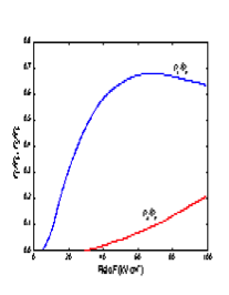
 | Frequency dependence of the efficiency η at first (solid line) and
at the second (dashed line) harmonic in LSA mode. Monte Carlo simulation. F = Fo + F1·sin(2π·ft) + F2·[sin(4π·ft)+3π/2], Fo=F1=35 kV cm-1, F2=10.5 kV cm-1 (Borodovskii and Osadchii [1987]). |
 | Longitudinal (D || F) and transverse (D ⊥ F) electron diffusion
coefficients at 300 K. Ensemble Monte Carlo simulation. (Aishima and Fukushima [1983]). |
 | Longitudinal (D || F) and transverse (D ⊥ F) electron diffusion
coefficients at 77K. Ensemble Monte Carlo simulation. (Aishima and Fukushima [1983]). |
Indium Phosphide (InP) is used to produce efficient lasers,
sensitive photodetectors and modulators in the wavelength window
typically used for telecommunications, i.e., 1550 nm wavelengths,
as it is a direct bandgap III-V compound semiconductor material.
The wavelength between about 1510 nm and 1600 nm has the lowest
attenuation available on optical fibre (about 0.26 dB/km). InP is a
commonly used material for the generation of laser signals and the
detection and conversion of those signals back to electronic form.
Wafer diameters range from 2-4 inches.
Applications are:
• Long-haul optical fibre connections over great distance up to
5000 km typically >10 Tbit/s
• Metro ring access networks
• Company networks and data center
• Fibre to the home
• Connections to wireless 3G, LTE and 5G base stations
• Free space satellite communication
Are You Looking for an InP substrate?
PAM-XIAMEN is proud to offer indium phosphide substrate for all different kinds of projects. If you are looking for InP wafers, send us enquiry today to learn more about how we can work with you to get you the InP wafers you need for your next project. Our group team is looking forward to providing both quality products and excellent service for you!