

Active Member
|
[China]

Address: #506B, Henghui Business Center, No.77, Lingxia Nan Road, High Technology Zone, Huli, Xiamen 361006, China
Contact name:

XIAMEN POWERWAY ADVANCED MATERIAL CO., LTD. |
|
|
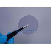
P Type , InP( Indium Phosphide) Substrate , 3”, Dummy Grade
PAM-XIAMEN provides single crystal InP(Indium phosphide) wafer for micro-electronic ( HBT/ HEMT ) and opto-electronic industry ( LED / DWDM / PIN / VCSELs ) in diameter up to 6 inch. Indium phosphide ( InP ) crystal is formed by two elements , Indium and Phosphide , growth by Liquid Encapsulated Czochralski ( LEC ) method or VGF method . InP wafer is an important semiconductor material which have superior electrical and thermal properties, InP wafer has higher electron mobility, higher frequency, low power consumption , higher thermal conductivity and low noise performance . PAM-XIAMEN can provide epi ready grade InP wafer for your MOCVD & MBE epitaxial application .
Please contact our engineer team for more wafer information.
P Type, InP Substrate, 3”, Dummy Grade
| 3"InP Wafer Specification | ||||
| Item | Specifications | |||
| Conduction Type | P-type | |||
| Dopant | Zinc | |||
| Wafer Diameter | 3" | |||
| Wafer Orientation | 100±0.5° | |||
| Wafer Thickness | 600±25um | |||
| Primary Flat Length | 16±2mm | |||
| Secondary Flat Length | 8±1mm | |||
| Carrier Concentration | ≤3x1016cm-3 | (0.8-6)x1018cm-3 | (0.6-6)x1018cm-3 | N/A |
| Mobility | (3.5-4)x103cm2/V.s | (1.5-3.5)x103cm2/V.s | 50-70cm2/V.s | >1000cm2/V.s |
| Resistivity | N/A | N/A | N/A | >0.5x10⁷Ω.cm |
| EPD | <1000cm-2 | <500cm-2 | <1x103cm-2 | <5x103cm-2 |
| TTV | <12um | |||
| BOW | <12um | |||
| WARP | <15um | |||
| Laser Marking | upon request | |||
| Suface Finish | P/E, P/P | |||
| Epi Ready | yes | |||
| Package | Single wafer container or cassette | |||
As we touched on in the introduction, Indium Phosphide is a semiconductor made of indium and phosphorus. It is used in high power and high-frequency electronics and has a high electron velocity. In fact, the electron velocity of InP is significantly higher than other more common semiconductors such as Silicon and Gallium Arsenide. It is also found in opto-electronic devices such as laser diodes.
| Breakdown field | ≈5·105 V cm-1 |
| Mobility electrons | ≤5400 cm2V-1s-1 |
| Mobility holes | ≤200 cm2 V-1s-1 |
| Diffusion coefficient electrons | ≤130 cm2 s-1 |
| Diffusion coefficient holes | ≤5 cm2 s-1 |
| Electron thermal velocity | 3.9·105 m s-1 |
| Hole thermal velocity | 1.7·105 m s-1 |
InP is used in high-power and high-frequency electronics[citation needed] because of its superior electron velocity with respect to the more common semiconductors silicon and gallium arsenide.
It was used with indium gallium arsenide to make a record breaking pseudomorphic heterojunction bipolar transistor that could operate at 604 GHz.
It also has a direct bandgap, making it useful for optoelectronics devices like laser diodes. The company Infinera uses indium phosphide as its major technological material for manufacturing photonic integrated circuits for the optical telecommunications industry, to enable wavelength-division multiplexing applications.
InP is also used as a substrate for epitaxial indium gallium arsenide based opto-electronic devices.
PAM-XIAMEN is your go-to place for everything wafers, including InP wafers, as we have been doing it for almost 30 years! Enquire us today to learn more about the wafers that we offer and how we can help you with your next project. Our group team is looking forward to providing both quality products and excellent service for you!
 Substrate , 3”, Dummy Grade")
 Substrate , 3”, Dummy Grade")
 Substrate , 3”, Dummy Grade")
 Substrate , 3”, Dummy Grade")
 Substrate , 3”, Dummy Grade")
 Substrate , 3”, Dummy Grade")