

Active Member
|
[China]

Address: #506B, Henghui Business Center, No.77, Lingxia Nan Road, High Technology Zone, Huli, Xiamen 361006, China
Contact name:

XIAMEN POWERWAY ADVANCED MATERIAL CO., LTD. |
|
|
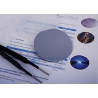
P Type , VGF InP Wafer With Single Or Double Side Polished , 2”, Test Grade
PAM-XIAMEN manufactures high purity single crystal Indium Phosphide Wafers for optoelectronics applications. Our standard wafer diameters range from 25.4 mm (1 inch) to 200 mm (6 inches) in size; wafers can be produced in various thicknesses and orientations with polished or unpolished sides and can include dopants. PAM-XIAMEN can produce wide range grades: prime grade, test grade, dummy grade, technical grade, and optical grade. PAM-XIAMEN also offer materials to customer specifications by request, in addition to custom compositions for commercial and research applications and new proprietary technologies.
P Type, InP Wafer, 2”, Test Grade
| 2"InP Wafer Specification | ||||
| Item | Specifications | |||
| Conduction Type | P-type | |||
| Dopant | Zinc | |||
| Wafer Diameter | 2" | |||
| Wafer Orientation | 100±0.5° | |||
| Wafer Thickness | 350±25um | |||
| Primary Flat Length | 16±2mm | |||
| Secondary Flat Length | 8±1mm | |||
| Carrier Concentration | ≤3x1016cm-3 | (0.8-6)x1018cm-3 | (0.6-6)x1018cm-3 | N/A |
| Mobility | (3.5-4)x103cm2/V.s | (1.5-3.5)x103cm2/V.s | 50-70cm2/V.s | >1000cm2/V.s |
| Resistivity | N/A | N/A | N/A | >0.5x10⁷Ωcm |
| EPD | <1000cm-2 | <500cm-2 | <1x103cm-2 | <5x103cm-2 |
| TTV | <10um | |||
| BOW | <10um | |||
| WARP | <12um | |||
| Laser Marking | upon request | |||
| Suface Finish | P/E, P/P | |||
| Epi Ready | yes | |||
| Package | Single wafer container or cassette | |||
Wafer Cleaning
Wafer cleaning is an integral part of the wafer industry. The cleaning process involves the removal of particulate and chemical impurities from the semiconductor. It’s imperative during the cleaning process that the substrate is not damaged in any way. Wafer cleaning is ideal for silicon-based materials since it’s the most common element that is used. Some of the benefits of wafer cleaning include:
Safely and effectively removes any surface
 | The dependence of ionization rates for electrons αi and holes βi
versus 1/F, 300 K. (Cook et al. [1982]). |
 | Breakdown voltage and breakdown field versus doping density for an
abrupt p-n junction, 300 K (Kyuregyan and Yurkov [1989]). |
Photovoltaic cells with highest efficiencies of up to 46% (Press Release, Fraunhofer ISE, 1. December 2014) implement InP substrates to achieve an optimal bandgap combination to efficiently convert solar radiation into electrical energy. Today, only InP substrates achieve the lattice constant to grow the required low bandgap materials with high crystalline quality. Research groups all over the world are looking for replacements due to the high costs of these materials. However, up to now all other options yield lower material qualities and hence lower conversion efficiencies. Further research focusses on the re-use of the InP substrate as template for the production of further solar cells.
Also today’s state-of-the-art high-efficiency solar cells for concentrator photovoltaics (CPV) and for space applications use (Ga)InP and other III-V compounds to achieve the required bandgap combinations. Other technologies, such as Si solar cells, provide only half the power than III-V cells and furthermore show much stronger degradation in the harsh space environment. Finally, Si-based solar cells are also much heavier than III-V solar cells and yield to a higher amount of space debris. One way to significantly increase conversion efficiency also in terrestrial PV systems is the use of similar III-V solar cells in CPV systems where only about one-tenth of a percent of the area is covered by high-efficiency III-V solar cells
Are You Looking for an InP substrate?
PAM-XIAMEN is proud to offer indium phosphide substrate for all different kinds of projects. If you are looking for InP wafers, send us enquiry today to learn more about how we can work with you to get you the InP wafers you need for your next project. Our group team is looking forward to providing both quality products and excellent service for you!


