

Active Member
|
[China]

Address: 深圳市宝安区福永凤凰西区202号信诺大厦401
Contact name:吴怡

Shenzhen Yideyi Technology Limited Company |
|
|
Multi PCB Types Manufacturer PCB Trading Companies PCB Soldering Service
Our services:
* Small to medium volume PCB manufacturer
* Multi PCB types manufacturer
* EMS/PCBA/OEM customers reliable PCB partner
* Trustworthy supplier for PCB trading companies
PCB capability:
| Specification | |
| Numbr of Layer | 1-18Layers |
| Material | FR-4,FR2.Taconic,Rogers, CEM-1 CEM-3,ceramic , crockery Metal-backed Laminate |
| Surface Finish | HASL(LF), Gold plating, Electroless nickel immersion gold, Immersion Tin, OSP(Entek) |
| Finish Board Thickness | 0.2mm-6.00 mm(8mil-126mil) |
| Copper Thickness | 1/2 oz min;12 oz max |
| Solder Mask | Green/Black/White/Red/Blue/Yellow |
| Min.Trace Width & Line Spacing | 0.075mm/0.1mm(3mil/4mil) |
| Min.Hole Diameter for CNC Driling | 0.1mm(4mil) |
| Min.Hole Diameter for punching | 0.9mm(35mil) |
| Biggest panel size | 610mm*508mm |
| Hole Positon | +/-0.075mm(3mil) CNC Driling |
| Conductor Width(W) | 0.05mm(2mil)or; +/-20% of original artwork |
| Hole Diameter(H) | PTH L:+/-0.075mm(3mil); Non-PTH L:+/-0.05mm(2mil) |
| Outline Tolerance | 0.125mm(5mil) CNC Routing; +/-0.15mm(6mil) by Punching |
| Warp & Twist | 0.70% |
| Insulation Resistance | 10Kohm-20Mohm |
| Conductivity | <50ohm |
| Test Voltage | 10-300V |
| Panel Size | 110×100mm(min);660×600mm(max) |
| Layer-layer misregistration | 4 layers:0.15mm(6mil)max; 6 layers:0.25mm(10mil)max |
| Min.spacing between hole edge to circuity pqttern of an inner layer | 0.25mm(10mil) |
| Min.spacing between board oulineto circuitry pattern of an inner layer | 0.25mm(10mil) |
| Board thickness tolerance | 4 layers:+/-0.13mm(5mil); 6 layers:+/-0.15mm(6mil) |
QUALITY:
All PCBs are 100% electrical tested. They can pick and send PCBs to
E-fixture test machines automatically, and place the PCBs at
appointed places after testing, according to the test result;All
PCBs are 100% visually inspected. All tests and inspect results are
recorded in the inspection report and shipped together with the
PCBs.
DIP capability:
• A-8 of semi-assembly work line with 3 set wave soldering machines
• B-4 of high/low-temperature burn-in test ovens for the burn-in tested required products
• All products are 100% inspected and tested during the DIP process

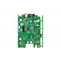
PCBA application:
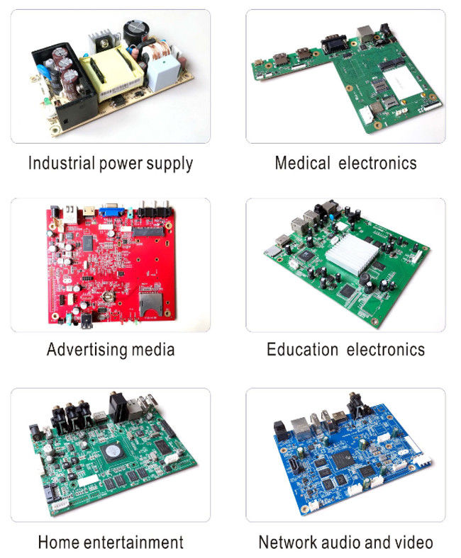
Shenzhen Yideyi Technology Co., Ltd professional engineers and technicians will work closely with you through our customer service people to ensure the best quality and quickest possible lead time.
FAQ:
Q1. How can we ensure our information should not let third party to
see our design?
We are willing to sign NDA effect by customer side local law and
promising to keep customers date in high confidential level in all
projects.
Q2. What service do you have?
We provide turnkey solution including RD, PCB fabrication, SMT,
final assembly,testing and other value-added service.
Q3. Please note that the following detail will speed up evaluation:
Material:
Board thickness:
Copper thickness:Surface finish:
Solder mask color:
Silkscreen color:
Q4. How about the delivery?
Normally, for sample order, our delivery is about 5 days.For small
batch, our delivery is about 7 days.
For mass production batch, our delivery is about 10 days.
But that depends on the real condition when we get your order.
If your order is urgently please contact us directly ,we will
priority to deal it and do ourbest to give you satisfied delivery
time.
Q5. With payment terms do we accept?
For sample order or small batch, we suggest you to use Pay-pal and
Western Union.For mass production batch, we suggest you to use T/T.
Q6. How can we guarantee you receive an good quality product?
For PCB, we will use Flying Probe Test, E-test etc. for it.
For PCBA, we need you to offer us a method or test fixture for the
function test.Before that, our inspectors will use microscope and
X-ray to check the IC footwelding or bad solder etc.


