Active Member
|
[China]

Address: Room 1520, Block 11, International E-Commerce Logistics Center, PingAn Road, PingHu Street, LongGang District, ShenZhen City, China 518111
Contact name:Steven YU

Witgain Technology Limited |
|
|
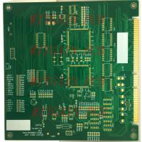
Gold Finger PCB 4 Layer Printed Circuit Board 1.6mm Thickness Green Solder Mask
Main Features:
1 4 Layer printed circuit board with gold fingers.
2 Gold thickness is 30U' on gold fingers.
3 FR4 sustrate material, tg170 degree.
4 Gold plating on gold fingers, for balance pads, we do immersion gold treatment.
5 1OZ finished cooper thickness on each layer.
6 Min line space and width is 5/5mil.
7 Drawing size is 280mm*172mm/1pcs.
8 ROHS, MSDS, SGS, UL, ISO9001&ISO14001 Certificated.
1 Consumer electronic products: SSD, TWS earphones, headsets,computer devices, portable power supplies, bluetooth modules, gps modules, wifi modules, smart keys for cars, intelligent locks, floor mopping robots, zigbee, etc.
2 Industrial control:main boards in machines, industrial robots, servo motors etc.
3 Automotive: BMS main boards, automotive radar etc.
4 Power supplies: UPS, industrial power supply, frequency power supply.
5 Medical: medical equipment, medical equipment power supply.
6 Communication products: 5G base station, routers, satellites, antennas.
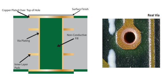
Q1: What is a Via?
A1: A Via is used to make an electrical connection between the layers of a Multi-Layer PCB. Connecting multiple layers of a board makes it possible to reduce the size of the PCB, as layers can be stacked. A via is constructed by placing copper pads on each layer of the PCB and drilling a hole through them. The hole is made conductive through electroplating or by placing copper cylinders directly in the drilled holes.
The inner part of the via is usually filled with a non-conductive material (air in most cases), while the outer layer of the cylinder has a conductive plating which is used to connect each layer of the PCB.
Note: It is always good to use multiple smaller vias rather than one large via since it reduces the inductance and also provides an additional path to the current flow in case any of the vias fail.
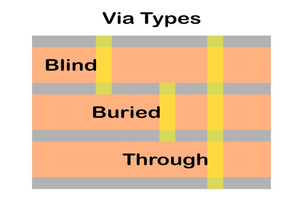
Types of Vias
There are three main types of Vias used in a Printed Circuit Board:
Through-Hole Via: This Via goes right through the PCB board from top to bottom and can be used to connect all the layers of a PCB. It is the most common via and is easiest to construct.
Blind Via: This Via connects the outermost layer of a PCB to the next layer. It can not be seen on the other side of the board and is therefore called blind via.
Buried Via: This Via can be used to connect internal layers of a PCB. It is not seen on the surface of the board.