Active Member
|
[China]

Address: Room 1520, Block 11, International E-Commerce Logistics Center, PingAn Road, PingHu Street, LongGang District, ShenZhen City, China 518111
Contact name:Steven YU

Witgain Technology Limited |

|
|
Gold Finger PCB FR4 BGA IPC ENIG 1u' 6 Layer PCB
PCB Specifications:
Part NO: 06B2105042
Layers: 6Layer
Surface Finished: Immersion gold 1u'
Material: FR4
Thickness: 1.6mm
PCB Size: 166.16mm*330mm
Finished copper: 1OZ
Solder Mask colour: Green
Silkscreen colour: White
No. of PP: 8pcs PP
Special Features: big size, Gold Finger with ENIG 1u' and solder mask ink plugged via hole
Standard: IPC-A-600G Class II
Certificates: UL/94V-0/ISO
Our Product Categories:
| Our Product Categories | ||
| Material Kinds | Layer Counts | Treatments |
| FR4 | Single Layer | HASL Lead Free |
| CEM-1 | 2 Layer/Double Layer | OSP |
| CEM-3 | 4 Layer | Immersion Gold/ENIG |
| Aluminum Substrate | 6 Layer | Hard Gold Plating |
| Iron Substrate | 8 Layer | Immersion Silver |
| PTFE | 10 Layer | Immersion Tin |
| PI Polymide | 12 Layer | Gold fingers |
| AL2O3 Ceramic Substrate | 14 Layer | Heavy copper up to 8OZ |
| Rogers, Isola high frequency materials | 16 Layer | Half plating holes |
| Halogen free | 18 Layer | HDI Laser drilling |
| Copper based | 20 Layer | Selective immersion gold |
| 22 Layer | immersion gold +OSP | |
| 24 Layer | Resin filled in vias | |
FAQ:
Q:Via hole plugging – what is it and when can it be used
A:

Are there different types of via hole plugging or protection? Are there variants when calling for a ‘plugged’ via? Yes there are. In fact there are seven types of via hole ‘protection’. Some are recommended and some are not, some are necessary for certain technologies, and all have different ‘names’. In this text, we will explain some of them.
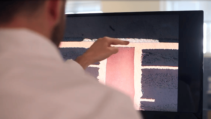
A via is a plated through hole (PTH) in a PCB that is used to provide electrical connection between a trace on one layer of the printed circuit board to a trace on another layer. Since it is not used to mount component leads, it is generally a small hole and pad diameter. The following are the two processes that can achieve this.
A via tenting is nothing more than covering its annular copper ring
with solder resist, also known as LPI (Liquid Photo Imageable) ink.
PCB designers need to remove the solder mask opening from its via
in their design, which enables via tenting. This is why it’s
considered standard and won’t increase the price of the PCB. In
this process, we can only ensure that the annular copper ring is
covered with solder resist ink. The surface of the hole may or may
not be covered with the solder resist ink. 
It is very important to note that the smaller the via hole size, the better the result will be. Suggested is a via >=0.20mm. Via hole sizes less than 0.3mm have the best chance of getting filled, while between 0.3mm to 0.5mm sizes, filling results may vary. Because this is an uncontrolled process, it is not recommended when holes need to be closed. Advantages:
Disadvantages:
Compared to tented vias, via holes are also filled with solder resist ink (LPI) in this process.

In this process, a drilled ALU sheet is used to push standard solder resist ink (LPI) into the via holes that need to be filled. The normal solder mask process is carried out after this screen printing process. 100% guaranteed result is assured in this process. Advantages:
Disadvantages:
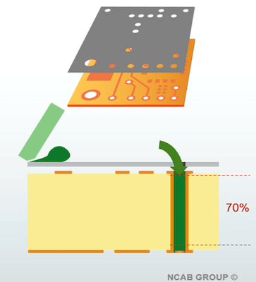
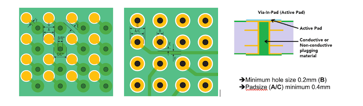
To manufacture products that are more and more compact and advanced, electronic engineers are facing a challenge to design circuit boards that are smaller without compromising performance. Therefore, BGA packages with smaller pitch or clearances are becoming more popular. Instead of using the standard “dog bone” footprint, where signals are transferred from the BGA pad to a via and then from the via to other layers, the via can be drilled directly into the BGA pad. This makes the routing of track work tighter and easier in designing PCBs as the surface of via itself becomes BGA pad allowing it to be treated as a normal SMD pad for soldering. This process is called “Via In Pad” while the pad is called an “Active Pad”.

Overall, there are two types of via plugging available depending on the material used in plugging process; non-conductive via plugging and conductive via plugging. Out of these two, the most common and widely preferable is non-conductive via plugging.
For PCB designs that require to transfer high amount of heat or current from one side of the board to another, conductive via plugging is a handy solution. It can also be used to dissipate excessive heat generated underneath some components. The metallic nature of the fill will naturally wick heat away from the chip to the other side of the board in many ways like a radiator. Advantages:
Disadvantages:
This is the most common and popular method of via plugging, especially for Via In Pad process. The barrel of via hole is filled with non-conductive material. Selection of the material depends on the CTE value, availability, specific design requirements and type of plugging machine. Thermal conductivity of non-conductive material is normally close to 0.25 W/mK. A common misconception about non-conductive via plugging is that the via will either not pass any current or only a weak electrical signal, which is absolutely not correct. The via will still be plated as normal before non-conductive material is plugged inside. It means via will work as normal as in any other standard PCB.
Advantages: