

Active Member
|
[China]

Address: 4113-4116# A Area, HSST PARK, BAO'AN District, Shenzhen, China
Contact name:Wendy

Abis Circuits Co., Ltd. |

|
|
ISO9001 Multilayer HDI PCB Board , 4/6/8 Layer Printed Circuit Board Immersion Gold 1OZ Finished Copper
HDI PCB Board Introduction
HDI PCB Board, also known as high-density interconnect PCB, is a kind of PCB with a higher wiring density per unit area than traditional boards. HDI boards are more compact and have smaller vias, pads, copper traces and spaces. As a result, HDIs have denser wiring resulting in lighter weight, more compact, lower layer count PCBs. HDI PCB is more fit into the little spaces and have a smaller amount of mass than conservative PCB designs.
Haina Lean provide One-stop PCB Board Favrication and assembly service , include :SMT Assembly , BGA Assembly , HDI ,Through-Hole Assembly ,Mixed Assembly,Rigid Flex PCB Assembly services . etc.
HDI PCB Detail Specifications
| Layers | 4 |
| Material | FR-4 |
| Board Thickness | 1.6mm |
| Copper Thickness | 2oz/70um |
| Surface Treatment | HASL Lead Free |
| Soldmask & Silkscreen | Blue&White |
| Quality Standard | IPC Class 2, 100% E-testing |
| Certificates | ISO14001, ISO9001, UL, cUL, TS16949 |
High Density PCB Capacity
| Layers | 1~20 |
| Board Thickness | 0.1mm-8.0mm |
| Material | FR4, CEM-1/CEM-3, PI, High Tg, Rogers, PTEF, Alu/Cu Base, etc |
| Max Panel Size | 600mm×1200mm |
| Min Hole Size | 0.1mm |
| Min Line Width/Space | 3mil(0.075mm) |
| Board Outline Tolerance | 0.10mm |
| Insulation Layer Thickness | 0.075mm--5.00mm |
| Out Layer Copper Thickness | 18um--350um |
| Drilling Hole (Mechanical) | 17um--175um |
| Finish Hole (Mechanical) | 0.10mm--6.30mm |
| Diameter Tolerance (Mechanical) | 0.05mm |
| Registration (Mechanical) | 0.075mm |
| Aspect Ratio | 16:01 |
| Solder Mask Type | LPI |
| SMT Mini. Solder Mask Width | 0.075mm |
| Mini. Solder Mask Clearance | 0.05mm |
| Plug Hole Diameter | 0.25mm--0.60mm |
| Impedance Control Tolerance | 10% |
| Surface finish | ENIG, OSP, HASL, Chem. Tin/Sn, Flash Gold |
| Soldermask | Green/Yellow/Black/White/Red/Blue |
| Silkscreen | Red/Yellow/Black/White |
| Certificate | UL, ISO 9001, ISO14001, IATF16949 |
| Special Request | Blind hole, Gold finger, BGA, Carbon ink, peelable mask, VIP process, Edge plating, Half holes |
| Material Suppliers | Shengyi, ITEQ, Taiyo, etc. |
| Common Package | Vacuum+Carton |
| FACTORY CAPABILITIES | |||
| No. | Items | 2019 | 2020 |
| 1 | HDI Capabilities | HDI ELIC (4+2+4) | HDI ELIC(5+2+5) |
| 2 | Max layer count | 32L | 36L |
| 3 | Board Thickness | Core thickness 0.05mm-1.5mm ,Fineshed board thickness 0.3-3.5mm | Core thickness 0.05mm-1.5mm ,Fineshed board thickness 0.3-3.5mm |
| 4 | Min.Hole Size | Laser 0.075mm Mechnical 0.15 | Laser 0.05mm Mechnical 0.15 |
| 5 | Min Line Width/Space | 0.035mm/0.035 | 0.030mm/0.030mm |
| 6 | Copper Thickness | 1/3oz-4oz | 1/3oz-6oz |
| 7 | Size Max Panel size | 700x610mm | 700x610mm |
| 8 | Registration Accuracy | +/-0.05mm | +/-0.05mm |
| 9 | Routing Accuracy | +/-0.075mm | +/-0.05mm |
| 10 | Min.BGA PAD | 0.15mm | 0.125mm |
| 11 | Max Aspect Ratio | 10:1 | 10:1 |
| 12 | Bow and Twist | 0.50% | 0.50% |
| 13 | Impedance Control Tolerance | +/-8% | +/-5% |
| 14 | Daily output | 3,000m2 (Max capacity of equipment) | 4,000m2 (Max capacity of equipment) |
| 15 | Surface Finishing | HASL Lead Free /ENEPING /ENIG /HASL /FINGER GOLD/IMMERSION TIN/SELECTIVE THICK GOLD | |
| 16 | Raw Material | FR-4/Normal Tg/High Tg/Low Dk/HF FR4/PTEE/PI | |
PCBA Capacity
| Capacity | |
| Single and double-sided SMT/PTH | Yes |
| Large parts on both sides, BGA on both sides | Yes |
| Smallest Chips size | 0201 |
| Min BGA and Micro BGA pitch and ball counts | 0.008 in. (0.2mm) pitch, ball count greater than 1000 |
| Min Leaded parts pitch | 0.008 in. (0.2 mm) |
| Max Parts size assembly by machine | 2.2 in. x 2.2 in. x 0.6 in. |
| Assembly surface mount connectors | Yes |
| Odd form parts: | Yes, Assembly by hands |
| LED | |
| Resistor and capacitor networks | |
| Electrolytic capacitors | |
| Variable resistors and capacitors (pots) | |
| Sockets | |
| Reflow soldering | Yes |
| Max PCB size | 14.5 in. x 19.5 in. |
| Min PCB Thickness | 0.2 |
| Fiducial Marks | Preferred but not required |
| PCB Finish: | 1. SMOBC/HASL |
| 2. Electrolytic gold | |
| 3. Electroless gold | |
| 4. Electroless silver | |
| 5. Immersion gold | |
| 6. Immersion tin | |
| 7. OSP | |
| PCB Shape | Any |
| Panelized PCB | 1. Tab routed |
| 2. Breakaway tabs | |
| 3. V-Scored | |
| 4. Routed+ V scored | |
| Inspection | 1. X-ray analysis |
| 2. Microscope to 20X | |
| Rework | 1. BGA removal and replacement station |
| 2. SMT IR rework station | |
| 3. Thru-hole rework station | |
| Firmware | Provide programming firmware files,Firmware + software installation instructions |
| Function test | Level of testing required along with test instructions |
| PCB file: | PCB Altium/Gerber/Eagle files (Including specs such as thickness, copper thickness, solder mask colour, finish, etc) |
| Category | Q/T Lead time | Standard Lead Time | Mass Production | |||
| 2 Layers | 24hrs | 3-4 working days | 8-15 working days | |||
| 4 Layers | 48hrs | 3-5 working days | 10-15 working days | |||
| 6 Layers | 72hrs | 3-6 working days | 10-15 working days | |||
| 8 Layers | 96hrs | 3-7 working days | 14-18 working days | |||
| 10 Layers | 120hrs | 3-8 working days | 14-18 working days | |||
| 12 Layers | 120hrs | 3-9 working days | 20-26 working days | |||
| 14 Layers | 144hrs | 3-10 working days | 20-26 working days | |||
| 16-20 Layers | Depends on the specific requirements | |||||
| 20+ Layers | Depends on the specific requirements | |||||
About us
Abis Circuits Co., Ltd is a professional PCB manufacturing which is focus on double side, Multilayer and HDI pcb mass production. The company was established on Oct,2006.we have two factories together ,The factory in Shenzhen is specialized in small to middle volume orders and the factory in shaoguan,GuangDong Province is for big volumn and HDI.
Nowadays we have more than 1100 employees over the two factories to cope with increasing demand.
Factory Operation plant space (I) 10000 Square meters
(II) 40000 Square Meters Employees
(III) 300 Man Powers (IV) 800 Man Powers Eng.Technical (V) 20 QA QC Engineers (VI) 60 QA,QC Engineers
Pre-Sale and After-Sale Service
1 Hour quotation
2 hours complaint feedback
7*24 hour technical support
7*24 order service
7*24 hour delivery
7*24 production run
Our Advantages
1, Single-sided PCB, double side & multi-layer PCB with competitive price, good quality, and excellent service.
2, CEM-1, CEM-3 FR-4, FR-4 High TG, Aluminum base material, Rogers, TEFLON
3, HASL, HASL lead free, Immersion Gold/ Silver/Tin, OSP, gold plating/finger, Carbon ink.
4, Printed Circuit Boards adhere to IPC Class 2 international PCB standard.
5, Factory audited by UL, IS09001/14001, SGS.
6, 100% E-Test.
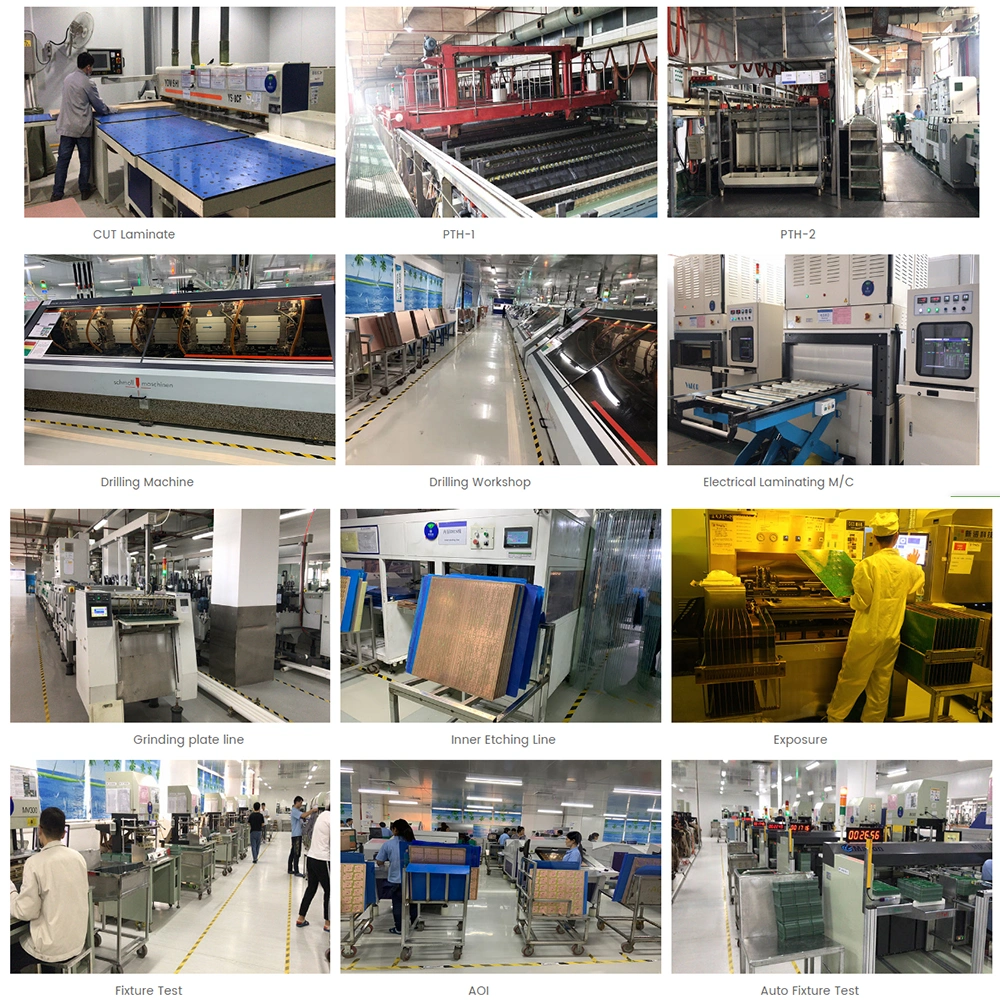
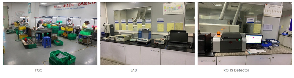
Factory overview
FAQ
Q: How about your delivery date ?
A: In general,smaples need 7 working days,mass production need 15-20 working days.
Q: What is your minimum order quantity?
A: NO MOQ.
Q: What is your advandage than other supplier ?
A: We have over 15 years experience in produce PCB services and have reliable of raw material suppliers. We can find out the best source to consistently reduce your cost.
Q: How about your supply capacity?
A: Our supply capacity is around 500000sqm each day.
Q: If No PCB file/Gerber file, only have the PCB sample,could you produce PCB board for me?
A: Yes, we could help you to clone the PCB board . Just send us the sample PCB , then produce for you. The cost depends on the PCB.
Q: Is safty for my PCB design for manufacturing?
A: All customer's copyright will never manufacture PCB board for someone else with your files unless we receive written.
Why choose us?
· With ABIS, customers significantly and effectively reduce their global procurement costs. Behind each service provided by ABIS, is hidden a cost saving for customers.
. We have two shop together, one is for prototype, quick turn, small volume making. The other is for mass production also for HDI board, with highly skilled professional employees, for high quality products with competitive price and on-time delivery.
. We provide very professional sales, technical and logistic supports, on a world-wide basis.hours complaint feedback.
ABIS cares every your order even 1 piece


