Active Member
|
[China]

Address: 4113-4116# A Area, HSST PARK, BAO'AN District, Shenzhen, China
Contact name:Wendy

Abis Circuits Co., Ltd. |

|
|
2 Oz High Density HDI PCB Board Programming Via In Pad HDI Circuit
Boards
Key HDI PCB Benefits
The evolution of PCB HDI technology has given engineers greater design freedom and flexibility than ever before. Designers using HDI high density interconnect methods now can place more components on both sides of the raw PCB if desired. In essence, an HDI PCB gives designers more space to work with, while allowing them to place smaller components even closer together. This means that a high-density interconnect PCB ultimately results in faster signal transmission along with enhanced signal quality.
HDI PCB is widely used to reduce the weight and overall dimensions
of products, as well as to enhance the electrical performance of
the device. The high-density PCB is regularly found in mobile
phones, touch-screen devices, laptop computers, digital cameras and
4G network communications. The HDI PCB is also prominently featured
in medical devices, as well as various electronic aircraft parts
and components. The possibilities for high-density interconnect PCB
technology seem almost limitless.
Company Profile
Abis Circuits Co., Ltd is a professional PCB manufacturer which was established on Oct, 2006 and focus on single side, double side, Multilayer and HDI pcb mass production.
Briefly introduce our strengths:
1. A professional PCB manufacturer which was established on Oct, 2006
2. Focusing on double side, Multilayer and HDI pcb mass production
3. Two factories, one for small and middle volume orders, another for
big volume and HDI
Quotation from ABIS
To ensure an accurate quote, be sure to include the following information for your project:
Your custom quote will be delivered in just 2-24 hours, depending on the design complexity.
Product Description
| Item | Production Capacity |
| Layer Counts | 1-20 layers |
| Material | FR-4,Cu base,High TG FR-4,PTFE,Rogers,TEFLON etc. |
| Board thickness | 0.20mm-8.00mm |
| Maximum Size | 600mmX1200mm |
| Board Outline Tolerance | +0.10mm |
| Thickness Tolerance(t≥0.8mm) | ±8% |
| Thickness Tolerance(t<0.8mm) | ±10% |
| Insulation Layer Thickness | 0.075mm--5.00mm |
| Minimum Line | 0.075mm |
| Minimum Space | 0.075mm |
| Out Layer Copper Thickness | 18um--350um |
| Inner Layer Copper Thickness | 17um--175um |
| Drilling Hole(Mechanical) | 0.15mm--6.35mm |
| Finish Hole(Mechanical) | 0.10mm-6.30mm |
| Diameter Tolerance(Mechanical) | 0.05mm |
| Registration(Mechanical) | 0.075mm |
| Aspect Ratio | 16:1 |
| Solder Mask Type | LPI |
| SMT Mini.Solder Mask Width | 0.075mm |
| Mini. Solder Mask Clearance | 0.05mm |
| Plug Hole Diameter | 0.25mm--0.60mm |
| Impedance control Tolerance | ±10% |
| Surface finish/treatment | HASL,ENIG,Chem,Tin,Flash Gold, OSP, Gold Finger |
PCB Capacity
| High precision prototype | PCB bulk production | ||
| Max Layers | 1-28 layers | 1-14 layers | |
| MIN Line width(mil) | 3mil | 3mil | |
| MIN Line space(mil) | 3mil | 3mil | |
| Min via (mechanical drilling) | Board thickness≤1.2mm | 0.15mm | 0.2mm |
| Board thickness≤2.5mm | 0.2mm | 0.3mm | |
| Board thickness>2.5mm | Aspect Ration≤13:1 | Aspect Ration≤13:1 | |
| Aspect Ration | Aspect Ration≤13:1 | Aspect Ration≤13:1 | |
| Board thickness | MAX | 8mm | 7mm |
| MIN | 2 layers:0.2mm;4 layers:0.35mm;6 layers:0.55mm;8 layers:0.7mm;10 layers:0.9mm | 2 layers:0.2mm;4 layers:0.4mm;6 layers:0.6mm;8layers:0.8mm | |
| MAX Board size | 610*1200mm | 610*1200mm | |
| Max copper thickness | 0.5-6oz | 0.5-6oz | |
Immersion Gold/ Gold Plated Thickness | Immersion Gold:Au,1—8u” Gold finger:Au,1—150u” Gold Plated:Au,1—150u” Nickel Plated:50—500u” | ||
| Hole copper thick | 25um 1mil | 25um 1mil | |
| Tolerance | Board thickness | Board thickness≤1.0mm:+/-0.1mm 1.0mm<Board thickness≤2.0mm:+/-10% Board thickness>2.0mm:+/-8% | Board thickness≤1.0mm:+/-0.1mm 1.0mm<Board thickness≤2.0mm:+/-10% Board thickness>2.0mm:+/-8% |
| Outline Tolerance | ≤100mm:+/-0.1mm 100<≤300mm:+/-0.15mm >300mm:+/-0.2mm | ≤100mm:+/-0.13mm 100<≤300mm:+/-0.15mm >300mm:+/-0.2mm | |
| Impedance | ±10% | ±10% | |
| MIN Solder mask bridge | 0.08mm | 0.10mm | |
| Plugging Vias capability | 0.25mm--0.60mm | 0.70mm--1.00mm | |
Lead Time
| Category | Quickest Lead Time | Normal Lead Time | |
| Double sideds | 24hrs | 120hrs | |
| 4 Layers | 48hrs | 172hrs | |
| 6 Layers | 72hrs | 192hrs | |
| 8 Layers | 96hrs | 212hrs | |
| 10 Layers | 120hrs | 268hrs | |
| 12 Layers | 120hrs | 280hrs | |
| 14 Layers | 144hrs | 292hrs | |
| 16-20 Layers | Depends on the specific requirements | ||
| Above 20 Layers | Depends on the specific requirements | ||
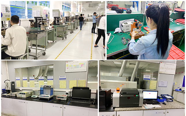
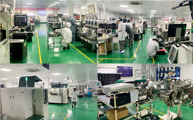
Factory