

Active Member
|
[China]

Address: 4113-4116# A Area, HSST PARK, BAO'AN District, Shenzhen, China
Contact name:Wendy

Abis Circuits Co., Ltd. |
|
|
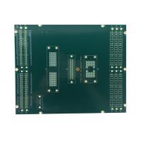
OSP/HASL/HASL-LF Prototype PCB Board in Green Ink with UL/ISO/IATF16949
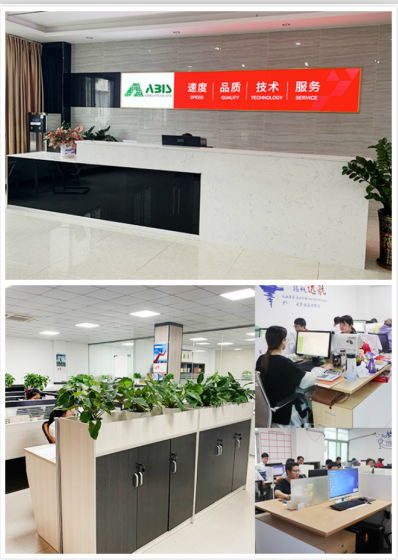
Company introduction
Abis Circuits Co., Ltd is a professional PCB manufacturer which was established on Oct, 2006 and focus on double side, Multilayer and HDI PCB mass production.
We have two factories together , the factory in Shenzhen is specialized in small and middle volume orders and the factory in Huizhou is for big volume and HDI. Our aim is help the clients gain more competitive strength and bring more mutual benefit to each other. All clients will be served well.
Factory
| Item | Production Capacity |
| Layer Counts | 1-20 layers |
| Material | FR-4,Aluminum Base,Cu base,High TG FR-4,PTFE,Rogers,TEFLON etc. |
| Board thickness | 0.20mm-8.00mm |
| Maximum Size | 600mmX1200mm |
| Board Outline Tolerance | +0.10mm |
| Thickness Tolerance(t≥0.8mm) | ±8% |
| Thickness Tolerance(t<0.8mm) | ±10% |
| Insulation Layer Thickness | 0.075mm--5.00mm |
| Minimum Line | 0.075mm |
| Minimum Space | 0.075mm |
| Out Layer Copper Thickness | 18um--350um |
| Inner Layer Copper Thickness | 17um--175um |
| Drilling Hole(Mechanical) | 0.15mm--6.35mm |
| Finish Hole(Mechanical) | 0.10mm-6.30mm |
| Diameter Tolerance(Mechanical) | 0.05mm |
| Registration(Mechanical) | 0.075mm |
| Aspect Ratio | 16:1 |
| Solder Mask Type | LPI |
| SMT Mini.Solder Mask Width | 0.075mm |
| Mini. Solder Mask Clearance | 0.05mm |
| Plug Hole Diameter | 0.25mm--0.60mm |
| Impedance control Tolerance | ±10% |
| Surface finish/treatment | HASL,ENIG,Chem,Tin,Flash Gold, OSP, Gold Finger |
Lead time
| Category | Quickest Lead time | Normal Lead Time | Mass Production | |||
| 2 Layers | 24hrs | 3-4 working days | 8-15 working days | |||
| 4 Layers | 48hrs | 3-5 working days | 10-15 working days | |||
| 6 Layers | 72hrs | 3-6 working days | 10-15 working days | |||
| 8 Layers | 96hrs | 3-7 working days | 14-18 working days | |||
| 10 Layers | 120hrs | 3-8 working days | 14-18 working days | |||
| 12 Layers | 120hrs | 3-9 working days | 20-26 working days | |||
| 14 Layers | 144hrs | 3-10 working days | 20-26 working days | |||
| 16-20 Layers | Depends on the specific requirements | |||||
| Above 20 Layers | Depends on the specific requirements | |||||
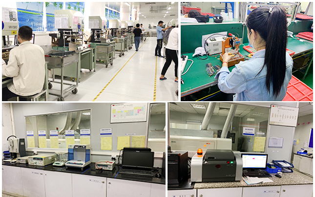
Manufacturing Equipment


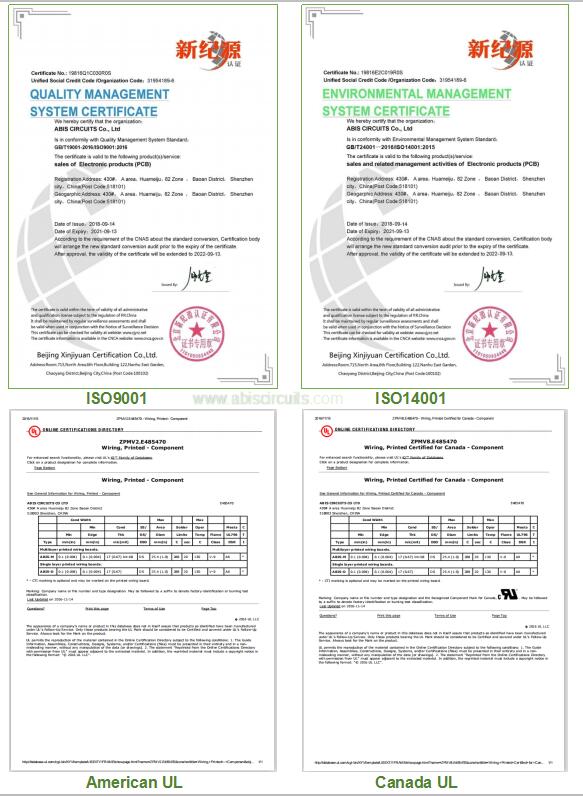
Certificate
FAQ
Q1:When can I get the quotation?
A:We usually quote with 1 hour after we get your inquiry. If you are
very urgent, please call us or tell us in your email.
Q2:Can you provide free samples for me?
A:Free samples depend on your order quantity.
Q3:I am a small wholesaler, do you accept small order?
A:It's no problem. If you're small wholesaler, we would like to grow
up with you together.
Q4:How many days will samples be finished? And how about the mass
production?
A:Generally 2-3 days for samples making. The lead time of mass
production will depend on the order quantity and the season you
place the order.
Q5:If I order big quantity, what's the good price?
A: Please send the details enquiry to us, such as the Item Number,
Quantity for each item, Quality request, Logo, Payment Terms,
Transport method, Discharge place etc. We will make the accurate
quotation to you as soon as possible.
Q6: How can we know the processing about PCB order?
A: Each Customer will have a sale to contact with you. Our working
hours: AM 9:00-PM 19:00(Beijing Time) from Monday to Friday. We
will reply your email as soon as quickly during our working time.
And you also could contact with our sales by cellphone if urgent.
Q7:Can I have samples to test?
A: Yes, we are pleased to supply module samples to test and check
quality, mixed sample order is available. Please note buyer should
pay for shipping cost.
Q8:Can you design pcb and make files for us?
A:yes,We have a professional drawing engineers' team that you can
trust.
Q9:If all pcb , PCBAs will be tested before delivery if we provide
the function testing method?
A:Yes, we ensure that each piece of pcb, PCBA will be tested before
shipment, we ensure the goods we sent with good quality
Q10:What is the shipping method?
A:We suggest you using DHL, UPS, FedEX, TNT forwarder.
Q11:How about the payment terms?
A:By T/T, Paypal, Western Union, etc.
Why choose us?
·With ABIS, customers significantly and effectively reduce their
global procurement costs. Behind each service provided by ABIS, is
hidden a cost saving for customers.
. We have two shop together, one is for prototype, quick turn, small
volume making. The other is for mass production also for HDI board,
with highly skilled professional employees, for high quality
products with competitive price and on-time delivery.
. We provide very professional sales, technical and logistic
supports, on a world-wide basis.hours complaint feedback.


