
|
|
[China]

Trade Verify
Address: Building C5/B6, Yanchuan North Industrial Park, Yanluo Street, Baoan District, Shenzhen, China
Contact name:Rachel

Shenzhen Benqiang Circuits Co,Ltd. |
|
Verified Suppliers
|
|
|
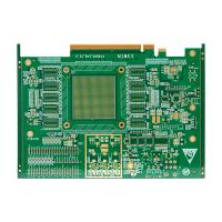
100% Testing and Er 3.48 Glass Epoxy HDI PCB Board for Consumer Electronics Industry
The HDI PCB Board is a high-density multilayer printed circuit board designed for use as a main board in a variety of electronic devices. With a thickness of 1.5 mm and a size of 300 * 210 mm, this board offers advanced interconnect solutions for a wide range of applications.
One of the key features of the HDI PCB Board is its high-density layered design. This allows for a greater number of components to be placed on the board, resulting in a more compact and space-efficient design. This is especially important for modern electronic devices, where miniaturization is a top priority.
The board also incorporates microvia technology, which involves the use of small, laser-drilled holes to create connections between different layers of the board. This allows for a higher density of interconnects, resulting in improved performance and reliability.
The HDI PCB Board is specifically designed for high-frequency applications, making it ideal for use in devices that require high-speed data transmission. The advanced interconnect solutions used in this board ensure high-frequency performance, making it a top choice for applications such as telecommunications, networking, and data storage.
To further enhance the performance and reliability of the board, it is finished with a chemical nickel palladium surface finish. This surface finish provides excellent corrosion resistance, ensuring the longevity of the board and its components. It also offers a smooth surface for easier soldering and improved signal integrity.
In summary, the HDI PCB Board is a high-density multilayer board that offers advanced interconnect solutions for main board applications. With its miniaturized design, microvia technology, and high-frequency performance, it is a top choice for modern electronic devices. The use of a chemical nickel palladium surface finish further enhances its reliability and performance, making it a reliable and efficient option for a wide range of applications.
| Specification | Value |
|---|---|
| Product Name | HDI PCB Board |
| Key Words | High Density Interconnector (HDI) |
| Alternate Name | Nanocircuit PCB, High Density Interconnection Printed Circuit Board |
| Impedance Control | Yes |
| Silkscreen Color | White, Black, Yellow, Red, Blue, Etc. |
| PCB Thickness | 1.5 mm |
| PCB Test | 100% Testing |
| Application | Main Board |
| Layer Count | 1-30 Layers |
| Board Size | 300 * 210 mm |
| Stencil Service | Yes |
| Number of Layers | 6-Layer |
The HDI PCB Board, also known as High Density Interconnector Printed Wiring Board, is a specialized type of PCB that is designed for high-density electronic devices. It utilizes advanced technologies such as microvia and nanocircuit to achieve a higher level of integration and performance. This product is widely used in various industries and applications, especially in main board designs.
The HDI PCB Board is an essential component in the design of main boards for electronic devices. Its compact size and high-density interconnects make it ideal for use in devices with limited space, such as smartphones, laptops, and tablets. The 6-layer design of the board allows for efficient routing of signals and power, making it suitable for complex main board designs.
The HDI PCB Board is also widely used in high-frequency applications, such as 5G communication devices, radar systems, and satellite communications. Its advanced design and materials enable it to handle high-frequency signals and maintain signal integrity, making it a popular choice for these applications.
The HDI PCB Board is known for its microvia technology, which allows for smaller vias and increased density of components on the board. This makes it ideal for use in high-speed and high-performance devices, as well as miniaturized electronic products. The microvia technology also enables the board to have a higher number of layers, making it suitable for more complex designs.
In addition to microvia technology, the HDI PCB Board also utilizes nanocircuit technology, which involves the use of very small conductive traces and spaces. This allows for a higher density of components and interconnects, as well as improved electrical performance. The nanocircuit technology makes the HDI PCB Board an ideal choice for advanced electronic devices, such as medical equipment and aerospace technology.
The HDI PCB Board is designed and manufactured with precision and undergoes 100% testing to ensure its reliability. This makes it a highly dependable product for critical applications that require high levels of accuracy and stability. The 6-layer design, along with the use of advanced technologies, also contributes to the board's durability and resistance to environmental factors.
The HDI PCB Board, with its advanced technologies and compact design, is a versatile and essential product for various electronic applications. Its high-density interconnects, microvia and nanocircuit technology, and 100% testing make it a reliable and high-performance choice for main board designs, high-frequency applications, and precision equipment. With its capabilities, the HDI PCB Board continues to play a crucial role in advancing the development of modern electronic devices.
At HDI PCB Board, we offer top-of-the-line customization services for our customers. Our high-density PCB panel and multilayer PCB technology allows for the creation of intricate and compact designs, perfect for nanocircuit PCB applications.
All of our products go through rigorous testing, ensuring that they meet the highest standards of quality and reliability. With our 100% testing guarantee, you can trust that your customized HDI PCB board will perform flawlessly.
Our immersion gold process creates a smooth and even surface, enhancing the conductivity and durability of our PCBs. With a thickness of 1.5 mm, our boards are sturdy and reliable, able to withstand the demands of various industries.
We offer customization for a variety of board sizes, including a standard size of 300 * 210 mm. Our 6-layer design allows for more complex and compact layouts, perfect for high-density and high-speed applications.
Choose HDI PCB Board for all your customization needs and experience the highest quality and reliability in every product. Contact us today to learn more about our services and how we can help bring your ideas to life.
At HDI PCB Board, we take pride in providing high-quality products to our customers. In order to ensure that your HDI PCB Boards arrive safely and in perfect condition, we have developed a thorough packaging and shipping process.
Our packaging process begins with carefully inspecting each HDI PCB Board to ensure that it meets our quality standards. Then, the boards are placed in anti-static bags to protect them from any potential damage during transportation. The bags are then placed in sturdy cardboard boxes and secured with bubble wrap to provide additional protection.
For larger orders, we use custom-made wooden crates to ensure maximum protection during shipping. Our crates are designed to withstand rough handling and are lined with foam to prevent any movement within the crate.
We offer a variety of shipping options to meet your needs. For domestic shipments, we use trusted carriers such as UPS, FedEx, and DHL. For international shipments, we work with major freight forwarders to ensure timely and secure delivery.
We also provide tracking information for all orders so that you can easily monitor the status of your shipment. If you have any specific shipping requirements, please let us know and we will do our best to accommodate them.
At HDI PCB Board, we understand the importance of timely delivery and we strive to meet all delivery deadlines. However, in the unlikely event that your order is delayed, we will keep you informed and work with you to find a suitable solution.
Thank you for choosing HDI PCB Board for your PCB needs. We are confident that our packaging and shipping process will ensure that your HDI PCB Boards arrive in perfect condition.


