
|
|
[China]

Trade Verify
Address: Building C5/B6, Yanchuan North Industrial Park, Yanluo Street, Baoan District, Shenzhen, China
Contact name:Rachel

Shenzhen Benqiang Circuits Co,Ltd. |
|
Verified Suppliers
|
|
|
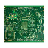
0.2mm-6.35mm Board Thickness High-speed PCB with Outline Rout And Score
| Technical Parameters | Value |
|---|---|
| Product Name | High Frequency PCB |
| Product Type | High-Frequency Microstrip PCB/High-Frequency Printed Wiring Board/High-speed PCB |
| Surface Finishing | ENIG (Electroless Nickel Immersion Gold) |
| Copper Thickness | 1 Oz |
| Minimum Via | 0.1mm Laser Drill, 0.2mm Mechanic Drill |
| Final Foil | 1 Oz |
| Outline | Rout And Score |
| Usage | OEM Electronics |
| Surface Finished | Immersion Gold |
| Board Thickness | 0.2mm-6.35mm |
| Impedance Value | ±10% |
| Board Thickness | 1.0MM |
The High Frequency PCB, also known as High-Frequency Microwave PCB, High-Frequency RF PCB, or High-Frequency Radio-frequency PCB, is a cutting-edge product designed to cater to the growing demand for high-speed and efficient communication and technology. It is a type of printed circuit board specifically designed to handle high-frequency signals and to provide low-loss transmission, making it a crucial component in various industries such as 4G/5G communication, aerospace technology, and medical equipment.
The High Frequency PCB boasts of several key attributes that make it stand out among other types of PCBs:
The High Frequency PCB is a versatile product that can be used in various applications and scenarios, including:
The High Frequency PCB has revolutionized the way we communicate and use technology, making it an essential component in various industries. Its high-frequency circuit design, low-loss materials, and ability to handle high-speed signals make it a game-changer in the world of electronics. With its reliability, efficiency, and compliance with environmental standards, the High Frequency PCB is truly a product of the future.
At High-Frequency PCB, we specialize in providing custom services for High-Frequency Radio-frequency PCB, High-Frequency Microstrip PCB, High-Frequency Stripline PCB, High-Frequency Hybrid PCB, and High-Frequency Millimeter Wave PCB. Our High-Frequency PCBs are designed to meet the specific needs of our clients in the communication and automotive industries.
Our High-Frequency PCBs are manufactured with a minimum hole size of 0.2mm, ensuring precise and accurate performance. The impedance value of our PCBs is maintained at ±10%, providing reliable and stable signal transmission. We use ENIG surface finishing, which offers excellent protection against oxidation and corrosion, making our PCBs suitable for long-term use in harsh environments.
Our High-Frequency PCBs are commonly used in communication and automotive applications where high-frequency signals are required. They are designed with Rogers or PTFE materials, which have excellent electrical properties and can withstand high temperatures, making them ideal for use in demanding environments.
At High-Frequency PCB, we understand the importance of customization in meeting the specific needs of our clients. Our team of experienced engineers and technicians work closely with our clients to understand their requirements and provide customized solutions to meet their unique needs. With our state-of-the-art equipment and advanced technology, we ensure the highest quality standards in every step of the production process.
Choose High-Frequency PCB for your custom High-Frequency PCB needs and experience superior quality, precision, and performance. Contact us today for a quote or to learn more about our services.
At High Frequency PCB, we take great care in packaging and shipping our products to ensure they arrive at your doorstep in perfect condition. Our packaging process follows industry standards and guidelines to guarantee the safety of your High Frequency PCB.
First, all High Frequency PCBs are inspected and tested before they are packaged. This ensures that only the highest quality products are shipped to our customers. The PCBs are then carefully placed in anti-static bags to prevent any damage from static electricity during transportation.
Next, the PCBs are placed in sturdy cardboard boxes with sufficient padding to protect them from any external impacts. The boxes are then sealed and labeled with the necessary information, such as product name, quantity, and shipping address.
We offer a variety of shipping options to meet your specific needs and budget. Our standard shipping method is through reputable international courier services, such as DHL, UPS, and FedEx. This ensures fast and reliable delivery to any location around the world.
For large orders or bulk shipments, we also offer sea freight or air freight services. Please contact us for a quote and estimated delivery time for these shipping options.
Please note that international orders may be subject to customs and duties fees upon arrival in your country. These fees are the responsibility of the customer and are not included in the shipping cost. We recommend checking with your local customs office for more information on these fees before placing your order.
For any questions or concerns about our packaging and shipping process, please don't hesitate to contact us. We are committed to providing you with the best service and ensuring your satisfaction with every High Frequency PCB you receive.


