
|
|
[China]

Trade Verify
Address: Building C5/B6, Yanchuan North Industrial Park, Yanluo Street, Baoan District, Shenzhen, China
Contact name:Rachel

Shenzhen Benqiang Circuits Co,Ltd. |
|
Verified Suppliers
|
|
|
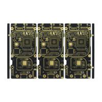
1.0MM Thickness High-Frequency Printed Circuit Board for OEM Electronics High-Frequency
High Frequency PCB, also known as High-speed PCB or High-Frequency Microstrip PCB, is a type of printed circuit board that is specially designed to handle high-frequency signals. This type of PCB is commonly used in applications such as communication and automotive industries, where high-speed and high-frequency signals are crucial for the proper functioning of electronic devices.
In conclusion, High Frequency PCBs are crucial components in high-speed, high-frequency electronic systems, offering excellent performance, reliability, and durability. With their specialized design and superior features, they are the preferred choice for applications in communication and automotive industries.
| Technical Parameters of High Frequency PCB | Specifications |
|---|---|
| Product Name | High Frequency PCB |
| Board Thickness | 0.2mm-6.35mm |
| Impedance Value | ±10% |
| Min Via | 0.1mm Laser Drill, 0.2mm Mechanic Drill |
| Minimum Hole Size | 0.2mm |
| Usage | OEM Electronics |
| Final Foil | 1 Oz |
| Surface Finished | Immersion Gold |
| Board Thk | 1.0MM |
| Rohs Compliant | Yes |
| Outline | Rout And Score |
| High-Frequency RF PCB | High-Frequency Stripline PCB |
| High-Frequency RF PCB Design | High-Frequency Stripline PCB Design |
The High Frequency PCB, also known as High-Frequency Printed Wiring Board, High-Frequency Microwave PCB, and High-Frequency Printed Circuit Board, is a type of printed circuit board that is specifically designed to meet the demands of high-frequency electronic devices. This type of PCB is made using specialized materials and processes to ensure high performance and reliability, even in extreme conditions.
The High Frequency PCB is widely used in various industries that require high-frequency electronic devices. Some of the common applications of this product are:
Imagine a high-tech laboratory where engineers are working on developing the latest medical equipment. One of the crucial components of this equipment is a high-frequency PCB, which is responsible for accurate and precise signal processing. The engineers are using specialized materials such as Rogers/PTFE and following strict manufacturing processes to ensure the quality and reliability of the PCB. The finished PCB is then integrated into the medical equipment, which goes through rigorous testing to ensure its performance in extreme conditions.
In another scenario, a team of engineers is designing a new communication system for a military aircraft. The system requires high-speed data processing and reliable signal transmission, which can only be achieved with the use of high-frequency PCBs. The engineers are carefully selecting the right board thickness and surface finishing, such as ENIG, to meet the demanding requirements of the aircraft. The finished PCB is then installed in the aircraft and is ready for use in critical missions.
From advanced medical equipment to cutting-edge military technology, the High Frequency PCB plays a vital role in various high-frequency electronic devices. Its ability to withstand extreme temperatures, provide high-speed signal processing, and maintain signal integrity makes it an essential component in today's technology-driven world.
Our High Frequency PCB is a high-quality, high-performance product designed for applications in the communication and automotive industries. It is specifically tailored to meet the demands of high-frequency signals and high-speed data transmission, making it an ideal choice for advanced electronic devices.
Our High Frequency PCB is suitable for a wide range of applications, including:
To order our High Frequency PCB, please provide the following specifications:
With our customizable board thickness options and high-frequency capabilities, our High Frequency PCB is the perfect choice for your next project. Contact us today to learn more!
High Frequency PCBs are delicate and require special packaging and shipping to ensure they arrive at their destination in perfect condition. Here are the steps we take to package and ship our High Frequency PCBs:
1. First, we carefully inspect each High Frequency PCB to ensure there are no defects or damage.
2. Next, we wrap the PCB in anti-static foam to protect it from electrostatic discharge during transport.
3. The wrapped PCB is then placed in a sturdy cardboard box with enough padding to prevent any movement during shipping.
4. If necessary, additional protective measures such as bubble wrap or packing peanuts may be used to further secure the PCB.
5. The box is then sealed and labeled with the necessary information for shipping.
1. We work with trusted shipping carriers to ensure safe and timely delivery of our High Frequency PCBs.
2. The PCBs are shipped using the appropriate method based on the size and weight of the package, as well as the destination.
3. Tracking information is provided to the customer so they can monitor the progress of their shipment.
4. Upon arrival, the package is carefully handled to prevent any damage during unloading.
5. If there are any concerns or issues with the PCB upon delivery, we have a dedicated customer service team ready to assist.
By following these packaging and shipping steps, we ensure that our High Frequency PCBs reach their destination in perfect condition, ready to be used in your high-tech applications.


