|
|
[China]

Trade Verify
Address: Address:Room624,Fangdichan development building,Guicheng south,Nanhai,Foshan,China
Contact name:Tracy

ONESEINE TECHNOLOGY CO.,LTD |
|
Verified Suppliers
|

|
|
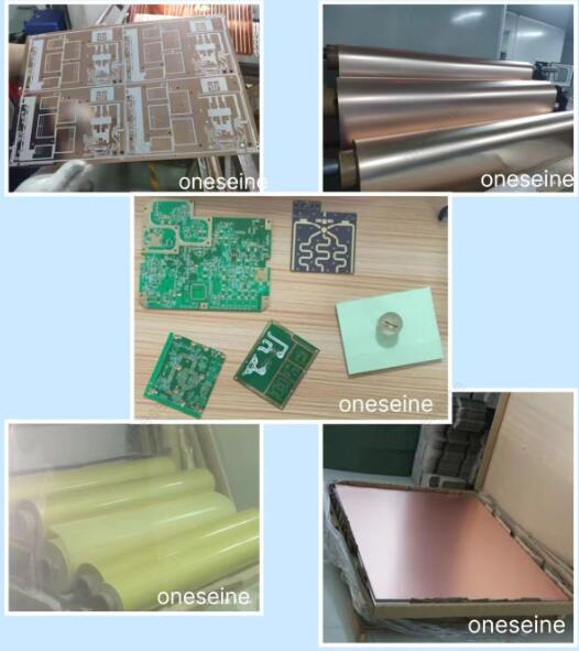
High Frequency Communication PCB Board Handling
PCB description:
Application Products: Power Amplifier
Number of layers: 2
Surface treatment: OSP
Material: ptfe f4b
PCB size:180*50mm
Outer line width/line spacing: 7/7mil
Inner line width/line spacing: 5/5mil
Board thickness: 2.3mm
Minimum aperture: 0.6mm
High frequency PCB range:
Frequency Range: High-frequency PCBs are designed to operate in frequency ranges typically starting from a few megahertz (MHz) and extending into the gigahertz (GHz) and terahertz (THz) ranges. These PCBs are commonly used in applications such as wireless communication systems (e.g., cellular networks, Wi-Fi, Bluetooth), radar systems, satellite communication, and high-speed data transmission.
Signal Loss and Dispersion: At high frequencies, signal loss and dispersion become significant concerns. High-frequency PCBs employ techniques to minimize these effects, such as using low-loss dielectric materials, controlled impedance routing, and minimizing the length and number of vias.
PCB Stackup: The stackup configuration of a high-frequency PCB is carefully designed to address signal integrity requirements. It typically consists of multiple layers of copper traces, dielectric materials, and ground planes. The arrangement of these layers is optimized to control impedance, minimize crosstalk, and provide shielding.
RF Connectors: High-frequency PCBs often incorporate specialized RF connectors to ensure proper signal transmission and minimize losses. These connectors are designed to maintain consistent impedance and minimize reflections.
Electromagnetic Compatibility (EMC): High-frequency PCBs must comply with electromagnetic compatibility standards to prevent interference with other electronic devices and to avoid susceptibility to external interference. Proper grounding, shielding, and filtering techniques are employed to address EMC requirements.
Simulation and Analysis: Designing high-frequency PCBs often involves simulation and analysis using specialized software tools. These tools allow designers to assess signal integrity, impedance matching, and electromagnetic behavior before fabrication, helping to optimize the PCB design for high-frequency performance.
Fabrication Challenges: Fabricating high-frequency PCBs can be more challenging compared to standard PCBs. The use of specialized materials, controlled impedance requirements, and tight tolerances require advanced fabrication techniques such as accurate etching, controlled dielectric thickness, and precise drilling and plating processes.
Testing and Validation: High-frequency PCBs undergo rigorous testing and validation to ensure their performance meets the desired specifications. This includes impedance testing, signal integrity analysis, insertion loss measurement, and other RF and microwave tests.
It's important to note that the design and manufacturing of high-frequency PCBs are specialized areas requiring expertise in RF and microwave engineering, PCB layout, and fabrication processes. Working with experienced professionals and consulting relevant design guidelines and standards is crucial to ensure reliable performance at high frequencies.
High frequency PCB description:
High frequency PCB material in stock:
| Brand | Model | Thickness(mm) | DK(ER) |
| Rogers | RO4003C | 0.203mm,0.305mm,0.406mm,0.508mm,0.813mm,1.524mm | 3.38 ± 0.05 |
| RO4350B | 0.101mm,0.168mm,0.254mm,0.338mm,0.422mm,0.508mm,0.762mm,1.524mm | 3.48 ± 0.05 | |
| RO4360G2 | 0.203mm,0.305mm,0.406mm,0.508mm,0.610mm,0.813mm,1.524mm | 6.15 ± 0.15 | |
| RO4835 | 0.168mm,0.254mm,0.338mm,0.422mm,0.508mm,0.591mm, 0.676mm,0.762mm,1.524mm | 3.48 ± 0.05 | |
| RT5870 | 0.127mm,0.787mm,0.254mm,1.575mm,0.381mm,3.175mm,0.508mm | 2.33 2.33 ± 0.02 | |
| RT5880 | 0.127mm,0.787mm,0.254mm,1.575mm,0.381mm,3.175mm,0.508mm | 2.20 2.20 ± 0.02 | |
| RO3003 | 0.13mm,0.25mm,0.50mm,0.75mm,1.52mm | 3.00 ±0.04 | |
| RO3010 | 0.13mm,0.25mm,0.64mm,1.28mm | 10.2 ± 0.30 | |
| RO3006 | 0.13mm,0.25mm,0.64mm,1.28mm | 6.15 ± 0.15 | |
| RO3203 | 0.25mm,0.50mm,0.75mm,1.52mm | 3.02±0.04 | |
| RO3210 | 0.64mm,1.28mm | 10.2±0.50 | |
| RO3206 | 0.64mm,1.28mm | 6.15±0.15 | |
| R03035 | 0.13mm,0.25mm,0.50mm,0.75mm,1.52mm | 3.50 ± 0.05 | |
| RT6002 | 0.127mm,0.254mm,0.508mm,0.762mm,1.524mm,3.048mm | 2.94 ± 0.04 | |
| RT6006 | 0.127mm,0.254mm,0.635mm,1.27mm,1.90mm,2.50mm | 6.15± 0.15 | |
| RT6010 | 0.127mm,0.254mm,0.635mm,1.27mm,1.90mm,2.50mm | 10.2 ± 0.25 | |
| TACONIC | TLX-8.TLX-9 | 0.508. 0.762 | 2.45-2.65 |
| TLC-32 | 0.254,0.508,0.762 | 3.35 | |
| TLY-5 | 0.254,0.508.0.8, | 2.2 | |
| RF-60A | 0.254.0.508.0.762 | 6.15 | |
| CER-10 | 0.254.0.508.0.762 | 10 | |
| RF-30 | 0.254.0.508.0.762 | 3 | |
| TLA-35 | 0.8 | 3.2 | |
| ARLON | AD255C06099C | 1.5 | 2.55 |
| MCG0300CG | 0.8 | 3.7 | |
| AD0300C | 0.8 | 3 | |
| AD255C03099C | 0.8 | 2.55 | |
| AD255C04099C | 1 | 2.55 | |
| DLC220 | 1 | 2.2 |