|
|
[China]

Trade Verify
Address: Address:Room624,Fangdichan development building,Guicheng south,Nanhai,Foshan,China
Contact name:Tracy

ONESEINE TECHNOLOGY CO.,LTD |
|
Verified Suppliers
|

|
|
High Frequency Arlon PCB For Power Divider / Coupler / Combiner
Quick detail:
Material: ArlonAD255,other rogers/Taconic/nelco material optional
Layer:2
Thickness:30mil
DK:2.55 DF:0.0018
Size: 8*6cm
Copper weight:2oz
Surface finish: Immersion gold
All hole PTH
Name: Arlon PCB,Power divider PCB manufacturer in China
Other arlon material:
Brand | Model | Thickness(mm) | DK(ER) | DF |
ARLON | AD255 | 0.762,1.5 | 2.55 | 0.0018 |
AD300C | 0.762.1.524 | 2.97 | 0.002 | |
TC350 | 0.254,0.762 | 3.5 | 0.002 | |
DiClad 522 | 0.508,0.787 | 2.4-2.6 | 0.0018 | |
DiClad 880 | 0.254,0.762 | 2.17 | 0.0009 | |
TC600 | 0.508,0.889 | 6.15 | 0.002 |
Power Divider PCB
Power divider, is a way to the input signal energy is divided into two or more output equal or unequal energy devices, but also in turn multi-channel signal energy output all the way, this May also be referred to as a combiner. A power divider between the output ports should ensure a certain degree of isolation. Power divider according to the output is usually divided into one into two (one input two outputs), one three (one input three output) and so on. The main technical parameters of the power splitter are power loss (including insertion loss, distribution loss and reflection loss), the voltage standing wave ratio of each port, the isolation between the power distribution ports, amplitude balance, phase balance, power capacity and frequency band Width and so on.
Power divider PCB can use rogers ,Taconic,Arlon or Isola high frequency material,it is according to your design,the most important is DK and DF ,thickness
You can inform me DK,DF and thickness,we can recommend relative material for your reference
Coupler PCB
In the microwave system, always need to be a way of microwave power divided into a few proportion, which is the power distribution problem. Components to achieve this function known as the power distribution components that coupler, including: directional coupler, power distributor and a variety of microwave branch devices.
Coupler PCB just a part of coupler,but it is most important than all
So Coupler PCB require high technology and material
We have more than 7 years manufacture experience of coupler pcb,so you can send us your design file and requirements here , we will quote you within 1 hours, if scarce material, then will within 1 day
Combiner PCB
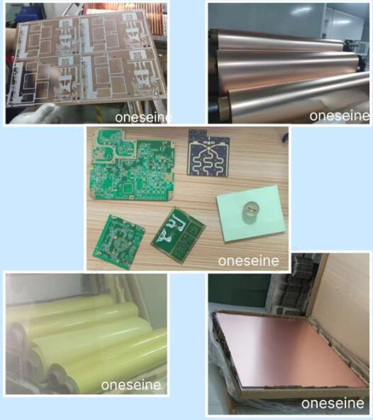
You can check our website for the detail pictures
High frequency PCB description:
High frequency PCB material in stock:
| Brand | Model | Thickness(mm) | DK(ER) |
| Rogers | RO4003C | 0.203mm,0.305mm,0.406mm,0.508mm,0.813mm,1.524mm | 3.38 ± 0.05 |
| RO4350B | 0.101mm,0.168mm,0.254mm,0.338mm,0.422mm,0.508mm,0.762mm,1.524mm | 3.48 ± 0.05 | |
| RO4360G2 | 0.203mm,0.305mm,0.406mm,0.508mm,0.610mm,0.813mm,1.524mm | 6.15 ± 0.15 | |
| RO4835 | 0.168mm,0.254mm,0.338mm,0.422mm,0.508mm,0.591mm, 0.676mm,0.762mm,1.524mm | 3.48 ± 0.05 | |
| RT5870 | 0.127mm,0.787mm,0.254mm,1.575mm,0.381mm,3.175mm,0.508mm | 2.33 2.33 ± 0.02 | |
| RT5880 | 0.127mm,0.787mm,0.254mm,1.575mm,0.381mm,3.175mm,0.508mm | 2.20 2.20 ± 0.02 | |
| RO3003 | 0.13mm,0.25mm,0.50mm,0.75mm,1.52mm | 3.00 ±0.04 | |
| RO3010 | 0.13mm,0.25mm,0.64mm,1.28mm | 10.2 ± 0.30 | |
| RO3006 | 0.13mm,0.25mm,0.64mm,1.28mm | 6.15 ± 0.15 | |
| RO3203 | 0.25mm,0.50mm,0.75mm,1.52mm | 3.02±0.04 | |
| RO3210 | 0.64mm,1.28mm | 10.2±0.50 | |
| RO3206 | 0.64mm,1.28mm | 6.15±0.15 | |
| R03035 | 0.13mm,0.25mm,0.50mm,0.75mm,1.52mm | 3.50 ± 0.05 | |
| RT6002 | 0.127mm,0.254mm,0.508mm,0.762mm,1.524mm,3.048mm | 2.94 ± 0.04 | |
| RT6006 | 0.127mm,0.254mm,0.635mm,1.27mm,1.90mm,2.50mm | 6.15± 0.15 | |
| RT6010 | 0.127mm,0.254mm,0.635mm,1.27mm,1.90mm,2.50mm | 10.2 ± 0.25 | |
| TACONIC | TLX-8.TLX-9 | 0.508. 0.762 | 2.45-2.65 |
| TLC-32 | 0.254,0.508,0.762 | 3.35 | |
| TLY-5 | 0.254,0.508.0.8, | 2.2 | |
| RF-60A | 0.254.0.508.0.762 | 6.15 | |
| CER-10 | 0.254.0.508.0.762 | 10 | |
| RF-30 | 0.254.0.508.0.762 | 3 | |
| TLA-35 | 0.8 | 3.2 | |
| ARLON | AD255C06099C | 1.5 | 2.55 |
| MCG0300CG | 0.8 | 3.7 | |
| AD0300C | 0.8 | 3 | |
| AD255C03099C | 0.8 | 2.55 | |
| AD255C04099C | 1 | 2.55 | |
| DLC220 | 1 | 2.2 |