XIAMEN POWERWAY ADVANCED MATERIAL CO., LTD. |
|
Undoped Gallium Antimonide Wafer, 3”, Polished Wafer, Epi Ready
PAM-XIAMEN manufactures high purity single crystal GaSb(Gallium Antimonide) Wafers Gallium antimonide (GaSb) is a semiconducting compound of gallium and antimony of the III-V family. It has a lattice constant of about 0.61 nm. It has a band gap of 0.67 eV. Our standard wafer diameters range from 1 inch to 4 inches, wafers can be produced in various thicknesses and different orientations (100),(111),(110) with polished wafers and blank wafers. PAM-XIAMEN can produce wide range grades: prime grade, test grade, dummy grade, mechanical grade, and optical grade. PAM-XIAMEN also offer GaSb material to customer specifications by request, in addition to custom compositions for commercial and research applications and new proprietary technologies.
3" GaSb Wafer Specification
| Item | Specifications |
| Conduction Type | P-type |
| Dopant | Undoped |
| Wafer Diameter | 3" |
| Wafer Orientation | (100)±0.5° |
| Wafer Thickness | 600±25um |
| Primary Flat Length | 22±2mm |
| Secondary Flat Length | 11±1mm |
| Carrier Concentration | (1-2)x1017cm-3 |
| Mobility | 600-700cm2/V.s |
| EPD | <2x103cm-2 |
| TTV | <12um |
| BOW | <12um |
| WARP | <15um |
| Laser marking | upon request |
| Suface finish | P/E, P/P |
| Epi ready | yes |
| Package | Single wafer container or cassette |
Band structure and carrier concentration of GaSb Wafer include
Basic Parameters,Mobility and Hall Effect,Transport Properties in
High Electric Fields
,Impact Ionization,Recombination Parameters
Basic Parameters
| Breakdown field | ≈5·104 |
| Mobility electrons | ≤ 3000 cm2 V-1 s-1 |
| Mobility holes | ≤ 1000 cm2 V-1 s-1 |
| Diffusion coefficient electrons | ≤ 75 cm2/s |
| Diffusion coefficient holes | ≤ 25 cm2/s |
| Electron thermal velocity | 5.8·105 m/s |
| Hole thermal velocity | 2.1·105 m/s |
 | Electron Hall mobility versus temperature for different doping
levels. 1. Nd= 1.7·1018 cm-3 2. Nd= 2.8·1017 cm-3 Broken curves represent the experimental data. Continuous curves represent theoretical calculations. |
 | Electron Hall mobility versus electron concentration no. T=77 K. Open circles represent measurements with a group of samples having approximately the same residual acceptor concentrations Na. Full symbols:specimens with lower residual acceptor concentrations. Solid lines represent the theoretical calculations for different values of compensating acceptor densities - either singly (Na-) or doubly (Na--) ionized. 1. Na- = 1.2·1017 or Na-- = 0.4·1017 cm-3 2. Na- =2.85·1017 or Na-- =0.95·1017 cm-3 3. Na- = 4.5·1017 or Na-- = 1.5·1017 cm-3 |
 | Hole Hall mobility versus temperature at different compensation
levels. 1. Na= 1.39·1017 cm-3; Nd= 9·1015 cm-3; 2. Na= 1.3·1017 cm-3; Nd= 9.5·1016 cm-3; 3. Na= 1.1·1017cm-3; Nd= 9.5·1016 cm-3 |
 | Temperature dependence of hole Hall mobility. MBE technique. Hole concentration at 300 K: 1. - 2.28·1016 cm-3; 2. - 1.9·1019 cm-3. |
 | The hole Hall mobility versus hole concentration, 300 K. Experimental data are taken from five different papers |
 | Calculated field dependence of the electron drift velocity, 300 K. |
 | Calculated (solid) end experimental (points) current density
dependencies versus the electric field, 300 K. |
 | Fraction of electrons in Γ, L, X valleys as a function of electric
field,300 K n=6.8·1016 cm-3 |
 | Electron temperature as a function of the electric field, T=77 K. full and open circle - experimental data curve are calculated |
 | The dependences of αi and βi> versus 1/F. T=77 K Open symbols : F (111). Filled symbols : F (100). |
 | The dependences of αi and βi versus 1/F). T=300 K F (100). |
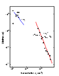
 | Radiative lifetime versus donor concentration, T =77 K, GaSb(Te). To extract these dependences from experimental data the values of internal quantum efficiency η were taken: open circles η=0.8; filled circles η=1; |
 | Nonradiative lifetime versus donor concentrations, T =77K,
GaSb(Te). open circles η= 0.8; filled circles η= 1; (Agaev et al. [1984]). |
 | Electron radiative (triangles) and nonradiative (squares) lifetime
versus acceptor concentration, p-GaSb, T=77 K. |
 | Electron lifetime versus temperature at different acceptor
concentrations. Na (cm-3): 1. 5·1018; 2. 2.2·1019; 3. 3.5·1019. |
| Radiative recombination coefficient | ~10-10 cm3 s-1 |
| Auger coefficient | |
| 77K | 2·10-29 cm6s-1 |
| 300 K | 5·10-30 cm6s-1 |
Are You Looking for an GaSb substrate?
PAM-XIAMEN is proud to offer Gallium antimonide substrate for all different kinds of projects. If you are looking for GaSb wafers, send us enquiry today to learn more about how we can work with you to get you the GaSb wafers you need for your next project. Our group team is looking forward to providing both quality products and excellent service for you!