

Active Member
|
[China]

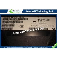
Address: Room 36B1-B2, Building C, Electronics Science & Technology Building Shennan Mid-Road, Shenzhen China
Contact name:Sharon Yang

Anterwell Technology Ltd. |
|
|
MC34063A, MC33063A, NCV33063A
1.5 A, Step−Up/Down/ Inverting Switching Regulators
The MC34063A Series is a monolithic control circuit containing the primary functions required for DC−to−DC converters. These devices consist of an internal temperature compensated reference, comparator, controlled duty cycle oscillator with an active current limit circuit, driver and high current output switch. This series was specifically designed to be incorporated in Step−Down and Step−Up and Voltage−Inverting applications with a minimum number of external components. Refer to Application Notes AN920A/D and AN954/D for additional design information.
Features
• Operation from 3.0 V to 40 V Input
• Low Standby Current
• Current Limiting
• Output Switch Current to 1.5 A
• Output Voltage Adjustable
• Frequency Operation to 100 kHz
• Precision 2% Reference
• Pb−Free Packages are Available
MAXIMUM RATINGS
Rating | Symbol | Value | Unit |
Power Supply Voltage | VCC | 40 | Vdc |
Comparator Input Voltage Range | VIR | −0.3 to +40 | Vdc |
Switch Collector Voltage | VC(switch) | 40 | Vdc |
Switch Emitter Voltage (VPin 1 = 40 V) | VE(switch) | 40 | Vdc |
Switch Collector to Emitter Voltage | VCE(switch) | 40 | Vdc |
Driver Collector Voltage | VC(driver) | 40 | Vdc |
Driver Collector Current (Note 1) | IC(driver) | 100 | mA |
Switch Current | ISW | 1.5 | A |
Power Dissipation and Thermal Characteristics |
|
|
|
Plastic Package, P, P1 Suffix |
|
|
|
TA = 25°C | PD | 1.25 | W |
Thermal Resistance | RθJA | 100 | °C/W |
SOIC Package, D Suffix |
|
|
|
TA = 25°C | PD | 625 | mW |
Thermal Resistance | RθJA | 160 | °C/W |
Operating Junction Temperature | TJ | +150 | °C |
Operating Ambient Temperature Range | TA |
| °C |
MC34063A |
| 0 to +70 |
|
MC33063AV, NCV33063A |
| −40 to +125 |
|
MC33063A |
| −40 to +85 |
|
Storage Temperature Range | Tstg | −65 to +150 | °C |
Stresses exceeding Maximum Ratings may damage the device. Maximum Ratings are stress ratings only. Functional operation above the Recommended Operating Conditions is not implied. Extended exposure to stresses above the Recommended Operating Conditions may affect device reliability.
1. Maximum package power dissipation limits must be observed.
2. This device series contains ESD protection and exceeds the following tests: Human Body Model 4000 V per MIL−STD−883, Method 3015. Machine Model Method 400 V.
3. NCV prefix is for automotive and other applications requiring site and change control.
Representative Schematic Diagram

MARKING DIAGRAMS PIN CONNECTIONS
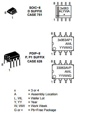

PACKAGE DIMENSIONS
SOIC−8 NB
D SUFFIX
CASE 751−07
ISSUE AG

PDIP−8
P, P1 SUFFIX
CASE 626−05
ISSUE L


