Active Member
|
[China]

Address: Room 36B1-B2, Building C, Electronics Science & Technology Building Shennan Mid-Road, Shenzhen China
Contact name:Sharon Yang

Anterwell Technology Ltd. |
|
|
MAX3232
3-V TO 5.5-V MULTICHANNEL RS-232 LINE DRIVER/RECEIVER
description
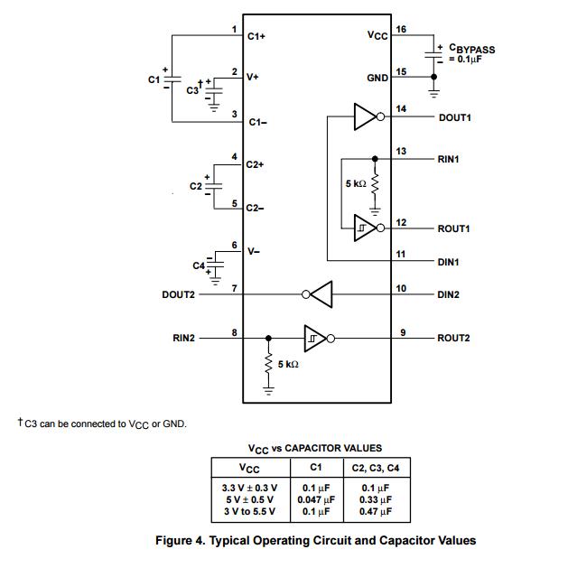
The MAX3232 device consists of two line drivers, two line receivers, and a dual charge-pump circuit with ±15-kV ESD protection pin to pin (serial-port connection pins, including GND). The device meets the requirements of TIA/EIA-232-F and provides the electrical interface between an asynchronous communication controller and the serial-port connector. The charge pump and four small external capacitors allow operation from a single 3-V to 5.5-V supply. The devices operate at data signaling rates up to 250 kbit/s and a maximum of 30-V/µs driver output slew rate.
The MAX3232C is characterized for operation from 0°C to 70°C. The MAX3232I is characterized for operation from –40°C to 85°C.
absolute maximum ratings over operating free-air temperature range
(unless otherwise noted)†
Supply voltage range, VCC (see Note 1) . . . . . . . . . . . . . . . . . . . . . . . . . . . . . . . . . . . . . . –0.3 V to 6 V
Positive output supply voltage range, V+ (see Note 1) . . . . . . . . . .. . . . . . . . . . . . . . . . . . –0.3 V to 7 V
Negative output supply voltage range, V– (see Note 1) . . . . . . . . . . . . . . . . . . . . . . . . . . .0.3 V to –7 V
Supply voltage difference, V+ – V– (see Note 1) . . . . . . . . . . . . . . . . . . . . . . . . . . . . . . . . . . . . . . 13 V
Input voltage range, VI : Drivers . . . . . . . . . . . . . . . . . . . . . . . . . . . . . . . . . . . . . . . . . . . . –0.3 V to 6 V
Receivers . . . . . . . . . . . . . . . . . . . . . . . . . . . . . . . . . . . . . . . . .. . –25 V to 25 V
Output voltage range, VO: Drivers . . . . . . . . . . . . . . . . . . . . . . . . . . . . . . . . . . . . . . . . –13.2 V to 13.2 V
Receivers . . . . . . . . . . . . . . . . . . . . . . . . . . . . . . . . . . –0.3 V to VCC + 0.3 V
Package thermal impedance, θJA (see Note 2): D package . . . . . . . . . . . . . . . . . . . . . . . . . . . .73°C/W
DB package . . . . . . . . . . . . . . . . . . . . . . . . . . . 82°C/W
DW package . . . . . . . . . . . . . . . . . . . . . . . . . . . .57°C/W
PW package . . . . . . . . . . . . . . . . . . . . . . . . . . .108°C/W
Lead temperature 1,6 mm (1/16 inch) from case for 10 seconds . . . . . .. . . . . . . . . . . . . . . . . . . . 260°C
Storage temperature range, Tstg . . . . . . . . . . . . . . . . . . . . . . . . . . . . . . . . . . . . . . . . . . –65°C to 150°C
† Stresses beyond those listed under “absolute maximum ratings” may cause permanent damage to the device. These are stress ratings only, and functional operation of the device at these or any other conditions beyond those indicated under “recommended operating conditions” is not implied. Exposure to absolute-maximum-rated conditions for extended periods may affect device reliability.
NOTES: 1. All voltages are with respect to network GND.
2. The package thermal impedance is calculated in accordance with JESD 51-7.
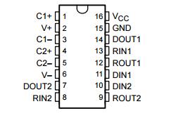
D, DB, DW, OR PW PACKAGE (TOP VIEW)
logic diagram (positive logic)

APPLICATION INFORMATION