

Active Member
|
[China]

Address: 深圳市宝安区福永凤凰西区202号信诺大厦401
Contact name:吴怡

Shenzhen Yideyi Technology Limited Company |
|
|
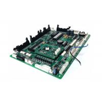
PCB Reverse Engineering Reproduction Static Flex Board Printed Board
We will reverse engineer your PCB sample, and submit the
engineering file into : PCB Gerber File,BOM List,Schematic
Diagram.
PCB reverse engineering is also known as PCB Copy, PCB cloning or
PCB duplication. It is a reversely researching technology based on
exisiting physical PCB boards.
| Reverse Engineering For Quote require | Sample for analysis | ||
| After Reverse Engineering what YDY provide? | 1. Gerber file,BOM list,IC decryption & software 4. Free samples | ||
| What I will required: | Images of PCB with components | Images without components |
PCB SMT Manufacture Capacity
| NO | Item | Technical capabilities |
| 1 | Layers | 1-20 layers |
| 2 | Max. Board size | 2000×610mm |
| 3 | Min. board Thickness | 2-layer 0.15mm |
| 4-layer 0.4mm | ||
| 6-layer 0.6mm | ||
| 8-layer 1.5mm | ||
| 10-layer 1.6~2.0mm | ||
| 4 | Min. line Width/Space | 0.1mm(4mil) |
| 5 | Max. Copper thickness | 10OZ |
| 6 | Min. S/M Pitch | 0.1mm(4mil) |
| 7 | Min. hole size | 0.2mm(8mil) |
| 8 | Hole dia. Tolerance (PTH) | ±0.05mm(2mil) |
| 9 | Hole dia. Tolerance (NPTH) | +0/-0.05mm(2mil) |
| 10 | Hole position deviation | ±0.05mm(2mil) |
| 11 | Outline tolerance | ±0.10mm(4mil) |
| 12 | Twist & Bent | 0.75% |
| 13 | Insulation Resistance | >10 12 Ω Normal |
| 14 | Electric strength | >1.3kv/mm |
| 15 | S/M abrasion | >6H |
| 16 | Thermal stress | 288°C 10Sec |

In order to reverse engineer a PCB, technicians start by examining and identifying the various components of the board. Each board will typically have resistors, capacitors, LEDs, a transistor, an inductor and various other features. The task here is to determine how the layout of these features gives the PCB its unique capabilities.
Before disassembly, the reverse-engineering team will photograph
the board up close from the front and back to create a record of
the board’s composition. Once the notes and images are collected,
the engineers begin the process of deconstructing the board.
YDY service:
1. PCBA, PCB assembly: SMT & PTH & BGA
2. PCBA and enclosure design
3. Components sourcing and purchasing
4. Quick prototyping
5. Plastic injection molding
6. Metal sheet stamping
7. Final assembly
8. Test: AOI, In-Circuit Test (ICT), Functional Test (FCT)
9. Custom clearance for material importing and product exporting
10. PCBA reverse engineering
11. Professtional R&D team
12. PCB Layout Design


