

Active Member
|
[China]

Address: 深圳市宝安区福永凤凰西区202号信诺大厦401
Contact name:吴怡

Shenzhen Yideyi Technology Limited Company |
|
|
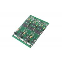
Immersion Silver Double Sided PCB Assembly Double Sided Placement
We provide:
1. Double Sided PCB Assembly
2. PCB fabrication
3. PCB design
4. ICT Testing
5. Thermal Profiling
6. PCBA production
7. Prototype made
8. PCBA engineering reserve
9. 3D printing
10. Electronics PCB Design
PCB capability:
| Specification | |
| Numbr of Layer | 1-16 Layers (standard) |
| Material | FR4, Aluminum, FPC |
| Surface Finish | HASL(LF), Gold plating, Enig,Immersion gold, Immersion Tin, OSP |
| Finish Board Thickness | 0.2mm-6.00 mm(8mil-126mil) |
| Copper Thickness | 1/2 oz min;12 oz max |
| Solder Mask | Green/Black/White/Red/Blue/Yellow |
| Min.Trace Width & Line Spacing | 0.075mm/0.1mm(3mil/4mil) |
| Min.Hole Diameter for CNC Driling | 0.1mm(4mil) |
| Min.Hole Diameter for punching | 0.9mm(35mil) |
| Biggest panel size | 610mm*508mm |
| Hole Positon | +/-0.075mm(3mil) CNC Driling |
| Conductor Width(W) | 0.05mm(2mil)or;+/-20% of original artwork |
| Hole Diameter(H) | PTH L:+/-0.075mm(3mil);Non-PTH L:+/-0.05mm(2mil) |
| Outline Tolerance | 0.125mm(5mil) CNC Routing;+/-0.15mm(6mil) by Punching |
| Warp & Twist | 0.70% |
| Insulation Resistance | 10Kohm-20Mohm |
| Conductivity | <50ohm |
| Test Voltage | 10-300V |
| Panel Size | 110×100mm(min);660×600mm(max) |
| Layer-layer misregistration | 4 layers:0.15mm(6mil)max;6 layers:0.25mm(10mil)max |
| Min.spacing between hole edge to circuity pattern of an inner layer | 0.25mm(10mil) |
| Min.spacing between board ouline to circuitry pattern of an inner layer | 0.25mm(10mil) |
| Board thickness tolerance | 4 layers:+/-0.13mm(5mil);6 layers:+/-0.15mm(6mil) |
| Impedance Control | +/-10% |
| Different Impendance | +-/10% |
Double-Sided PCB - The Most Popular Type of PCB in The Industry
While single-sided PCBs are ideal and straightforward to use when
possible, many circuits require two sides. Double-sided PCB boards
offer a wide variety of possibilities for circuit board designers
because they have more surface area and flexibility when routing
traces. Using two sides instead of one also allows for a smaller
board size overall, which can be important when building
small-scale, integrated devices. Double-sided PCB is one of the
most common types of PCBs. Moreover, the two-sided PCB and the
single-sided PCB are the same to some extent.
The difference is that the single-sided PCB has only one conductive surface. That is to say, the single PCB has copper on one side of the board, but the two-sided PCB has a conductive layer on each side. The dielectric layer is surrounded by the copper layer of the circuit and welding masks on both sides. Technically, single-sided circuit boards will not be copper plated in boreholes. Passing holes allow manufacturers to create traces on both sides that are adjacent to each other and connected between layers.
PCB manufacturers use double-sided PCBs for products that require elementary to intermediate circuit complexity. This type of PCB does not provide as much circuit complexity or density as multi-layer PCB, but it is the most economical choice in many applications.
Double Sided PCA case
Shenzhen Yideyi Technology Co., Ltd. according to customer demand
for the domestic and foreign relevant industry to provide technical
research and development, product design and solution services.

FAQ:
Q1. How can we ensure our information should not let third party to
see our design?
We are willing to sign NDA effect by customer side local law and
promising to keep customers date in high confidential level in all
projects.
Q2. What service do you have?
We provide turnkey solution including RD, PCB fabrication, SMT,
final assembly,testing and other value-added service.
Q3. Please note that the following detail will speed up evaluation:
Material:
Board thickness:
Copper thickness:Surface finish:
Solder mask color:
Silkscreen color:
Q4. How about your factory production capacity?
we can provide 30000 square meter/month.
Q5. With payment terms do we accept?
For sample order or small batch, we suggest you to use Pay-pal and
Western Union.For mass production batch, we suggest you to use T/T.
Q6. How can we guarantee you receive an good quality product?
For PCB, we will use Flying Probe Test, E-test etc. for it.
For PCBA, we need you to offer us a method or test fixture for the
function test.Before that, our inspectors will use microscope and
X-ray to check the IC footwelding or bad solder etc.
Q7. What are the main products of your PCB/PCBA service?
Automotive, medical, Industrial control, Internet of Things, Smart home, military, Aerospace.
Q8. What payment do you accept ?
T/T, L/C, D/P, D/A etc.


