
|
|
[China]

Trade Verify
Address: Room 502, 26# Building, Funing Hi-Tech Industrial Park, Fuhai Street, Bao'an, Shenzhen, Guangdong, China, 518103
Contact name:Helen Jiang

Shenzhen KAZ Circuit Co., Ltd |
|
Verified Suppliers
|
|
|
Electronic Manufacturing Service Quick Turn PCB Assembly
Detail Specifications:
| Layers | 6 |
| Material | FR-4 |
| Board Thickness | 1.6mm |
| Copper Thickness | 1oz |
| Surface Treatment | ENIG |
| Soldmask & Silkscreen | Green |
| Quality Standard | IPC Class 2, 100% E-testing |
| Certificates | TS16949, ISO9001, UL, RoHS |
What KAZ Circuit can do for you:
To get a full quotation of the PCB/PCBA, pls provide the
information as below:
Company Informaiton:
KAZ Circuit is a professional PCB manufacturer from China since
2007, also provide PCB Assembly service for our customers. Now with
about 300 employees. Certified with ISO9001,TS16949, UL, RoHS. We
are confident to provide you quality products with factory-directed
price within the fastest delivery time!
Manufacturer Capacity:
| Capacity | Double Sided: 12000 sq.m / month Multilayers: 8000sq.m / month |
| Min Line Width/Gap | 4/4 mil (1mil=0.0254mm) |
| Board Thickness | 0.3~4.0mm |
| Layers | 1~20 layers |
| Material | FR-4, Aluminum, PI |
| Copper Thickness | 0.5~4oz |
| Material Tg | Tg140~Tg170 |
| Max PCB Size | 600*1200mm |
| Min Hole Size | 0.2mm (+/- 0.025) |
| Surface Treatment | HASL, ENIG, OSP |
SMT Capacity

Prototype PCB assembly refers to the process of assembling and
manufacturing a small batch or a single prototype printed circuit
board (PCB). This process involves soldering electronic components
onto the PCB to create a functional electronic circuit.
Here are the general steps involved in prototype PCB assembly:
PCB Design: The first step is to design the PCB layout using
software tools like EDA (Electronic Design Automation) software.
The design includes placing components, creating traces, and
defining the PCB's dimensions.
Gerber File Generation: After the PCB design is complete, a Gerber
file is generated. The Gerber file contains all the necessary
information about the PCB layout, including the component
placement, copper traces, drill holes, and solder mask.
Component Procurement: Once the Gerber files are ready, you need to
procure the required electronic components for the assembly. This
involves sourcing the components from suppliers or distributors.
It's essential to ensure that you have the correct components and
necessary quantities for the prototype.
PCB Fabrication: The Gerber files are sent to a PCB fabrication
service or manufacturer to produce the actual PCB. The manufacturer
creates the PCB by etching the copper layers, applying solder mask,
and drilling holes according to the design specifications.
Stencil Creation: A stencil is used for applying solder paste onto
the PCB before component placement. The stencil is typically made
of metal and has openings for each surface-mount component's solder
pads.
Solder Paste Application: Solder paste, a sticky mixture of tiny
solder balls and flux, is applied to the PCB using the stencil. The
solder paste is applied to the designated soldering pads for each
component.
Component Placement: The components are then placed on the solder
paste, either manually or using automated pick-and-place machines.
The pick-and-place machine uses a vacuum nozzle to pick up each
component from a reel or tray and accurately places it on the
solder paste.
Soldering: After component placement, the PCB is subjected to a
reflow soldering process. The entire assembly is heated to a
specific temperature to melt the solder paste, creating a permanent
mechanical and electrical connection between the components and the
PCB.
Inspection and Testing: Once the soldering process is complete, the
PCB assembly undergoes quality inspection to ensure that all
components are correctly placed and soldered. Visual inspection,
automated optical inspection (AOI), or X-ray inspection is
performed to detect any defects. The assembled PCB is then tested
to verify its functionality.
Rework and Debugging: If any issues are identified during
inspection or testing, rework may be required. This involves fixing
any problems, such as re-soldering components or correcting
soldering defects. Debugging may also be necessary to troubleshoot
and resolve any functional issues.
Finalization: Once the prototype PCB assembly passes inspection and
testing, it is considered ready for further evaluation or
integration into a larger system.
It's worth noting that the specific details of the prototype PCB
assembly process may vary depending on factors such as the
complexity of the design, the size of the PCB, and the available
manufacturing resources.
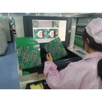
Photoes of Electronic Manufacturing Service Quick Turn PCB Assembly Service


