Active Member
|
[China]

Address: Room 1520, Block 11, International E-Commerce Logistics Center, PingAn Road, PingHu Street, LongGang District, ShenZhen City, China 518111
Contact name:Steven YU

Witgain Technology Limited |

|
|
4 Layer PCB Half Hole 1.0 MM Thickness Immersion Gold HDI PCB
Board Info:
1 Part NO: Half hole PCB0010
2 Layer Count: 4 Layer PCB
3 Finished Board Thickness: 1.0 MM tolerance is +/-0.1MM
4 Solder Mask: Green
5 Min Lind Space&Width: 4/4 mil
6 Application Area: Blue-tooth Module
7 Drillings: L1-L2 0.1MM Laser drilling, L3-L4 0.1MM Laser Drilling, L1-L4 0.2MM Mechanical Drilling
8 BGA Size: 0.2MM, Laser drilling on BGA PAD and plated flat
9 Surface Treatment: immersion gold + osp
10 PCB Size: 109.6mm*82mm/20pcs
11 Impedance control: 50 ohm and 100 ohm
X-OUT per panel:
1 X-OUT panel must be packed separately and marked clearly
2 A black X must be permanently marked on both sides of pcb
3 X-OUT per panel not be over 25%
4 X-OUT per lot not be over 5%
FAQ:
Q1: What is an Annular Ring?
A1: A via is created by drilling a hole through a copper pad etched on each layer of a PCB. An Annular Ring is the area between the edge of the drilled via and the copper pad associated with that hole. The greater the width of an annular ring, the greater the copper connection around the drilled via will be.
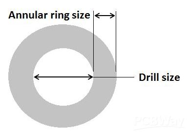
In a multilayer PCB, traces are routed from one layer to another layer with the help of vias. These vias are the holes drilled through copper pads on the surface of the PCB. The amount of copper left around the via on both top and bottom sides of the PCB is called the annular ring.
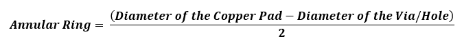
Mathematically, an annular ring is the difference between the diameter of the hole and diameter of the pad divided by 2. For instance, if the diameter of the pad is 24 mils and the diameter of the hole is 12 mils then the width of the annular ring is [(24-12)/2] = 6 mils
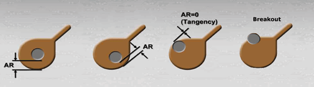
Calculation of the width of an annular ring plays an important role at the time of PCB manufacturing. If the width of the annular ring is not enough then the hole could touch the boundaries of the pad, this condition is called ‘Tangency’. In the extreme situation, the hole could be outside the boundary of the pad which is termed as ‘Breakout’. Both these situations should be avoided during the process of PCB fabrication.