

Active Member
|
[China]

Address: Room 1520, Block 11, International E-Commerce Logistics Center, PingAn Road, PingHu Street, LongGang District, ShenZhen City, China 518111
Contact name:Steven YU

Witgain Technology Limited |
|
|
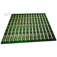
4 Layer PCB 1.2 MM Thickness Used In TWS Earphone
1 4 Layer Printed Circuit Board PCB .
2 Immersion Gold treatment, gold thickness 1u'.
3 FR4 substrate material, tg130 degree.
4 Min line space and width 6/6 mil.
5 Copper thickness is 1 oz on each layer, 35 um on each layer.
6 Green solder mask and white silkscreen.
7 ROHS, MSDS, SGS, UL, ISO9001&ISO14001 Certificated
| Our Product Categories | ||
| Material Kinds | Layer Counts | Treatments |
| FR4 | Single Layer | HASL Lead Free |
| CEM-1 | 2 Layer/Double Layer | OSP |
| CEM-3 | 4 Layer | Immersion Gold/ENIG |
| Aluminum Substrate | 6 Layer | Hard Gold Plating |
| Iron Substrate | 8 Layer | Immersion Silver |
| PTFE | 10 Layer | Immersion Tin |
| PI Polymide | 12 Layer | Gold fingers |
| AL2O3 Ceramic Substrate | 14 Layer | Heavy copper up to 8OZ |
| Rogers, Isola high frequency materials | 16 Layer | Half plating holes |
| Halogen free | 18 Layer | HDI Laser drilling |
| Copper based | 20 Layer | Selective immersion gold |
| 22 Layer | immersion gold +OSP | |
| 24 Layer | Resin filled in vias | |
Q1: What is a PCB Test Coupon?
A1: During the PCB Manufacturing process, it is important to evaluate the quality of the boards being fabricated. A good way to do this is to fabricate a few extra boards called PCB Test Coupons which can be tested to evaluate the performance of the boards. PCB Test Coupons are designed to have the same spec (trace width, copper weight, via structure, etc.) as the original PCB board and are tested to identify manufacturing defects, material defects or other related defects.
During the PCB Fabrication process multiple PCBs are fabricated on a large board called a panel. The PCB Test Coupon is usually not a part of the core PCB panel, is built in section surrounding the PCBs. They are designed to represent actual board conditions for plating, etching and lamination. It's common to fabricate one coupon at each end of a board panel to verify performance across the entire panel. Any defect identified in the PCB Test Coupon would mean that other boards on the same panel would have the same issues.
Advantages of using PCB Test Coupon:


