

Active Member
|
[China]

Address: Room 1520, Block 11, International E-Commerce Logistics Center, PingAn Road, PingHu Street, LongGang District, ShenZhen City, China 518111
Contact name:Steven YU

Witgain Technology Limited |
|
|
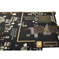
6 Layer PCB Display Screen Used Black Solder Mask
Printed Circuit Board Features:
1 6 Layer printed circuit board used in display screen.
2 FR4 substrate material, tg 150 degree and board thickness is 2.0mm.
3 Black solder mask and white silkscreen.
4 OSP Treatment
5 PCB size is 748mm*90.4mm/1pcs.
6 35 um copper thcikness on each layer.
7 PCB file or gerber file should be offered by customer.
8 Customized printed circuit board.
Our history:

A grid testing machine has three building blocks - a fixture, a bed of nails and software, to control the overall functionality of the machine. It usually has two cameras which are placed on the top and bottom of the machine in order to scan the whole board.
Advantages of PCB Grid Testing:
Limitations of PCB Grid Testing:
This type of testing is called In-Circuit Testing. Another test process used for In-Circuit testing is Flying Probe Testing.


