

Active Member
|
[China]

Address: Room 1520, Block 11, International E-Commerce Logistics Center, PingAn Road, PingHu Street, LongGang District, ShenZhen City, China 518111
Contact name:Steven YU

Witgain Technology Limited |
|
|
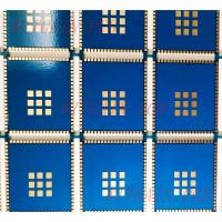
8 Layer PCB Used In GPS Module Blue Solder Mask ENIG
Main Features:
1 8 Layer Printed Circuit Board with very high relability.
2 PCB drawing size is 118.8mm*115mm/12pcs
3 Copper thickness is 35 um on each layer
4 FR4 substrate material ,TG150 degree.
FAQ:
Q1:What is PCB Grid Testing or Bed of Nails Testing?
A1: Grid testing or Bed of Nails testing is a process used to check the performance of components mounted on a PCB board. This test uses a frame/fixture that contains various pins inserted into an epoxy phenolic glass cloth laminated sheet (G-10) in order to access all the PCB test points. These pins act as sensors which are aligned to make contact with the test points on the PCB board and are also connected with a measuring unit through wires. The position of the pins is designed and customized for each PCB based on the components or points on the board that need to be tested.

Limitations of PCB Grid Testing:
This type of testing is called In-Circuit Testing. Another test process used for In-Circuit testing is Flying Probe Testing.


