

Active Member
|
[China]

Address: Room 1520, Block 11, International E-Commerce Logistics Center, PingAn Road, PingHu Street, LongGang District, ShenZhen City, China 518111
Contact name:Steven YU

Witgain Technology Limited |
|
|
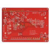
Printed Circuit Boards 4 Layer PCB In Red Solder Mask And OSP Treatment
Specifications:
1 All dimensions are in MM.
2 Fabricate per IPC-6012A Class2.
3 Materials:
3.1 Dielectric: FR4 Per IPC or equivalent
3.2 Min Tg: 170DEG
3.3 Copper: As per stack up
3.4 UL Rating: 94V0 Minimum
4 Surface finish: ENIG
5 Solder mask material should meet all requirement of the IPC-SM-840E and shall be green in color and applied over bare copper. Vendor may edit solder mask and paste mask as needed.
6 Editing of existing copper layers shall require customer approval.
7 Silkscreen legend to be applied per layer stackup using white non-conductitive epoxy ink.
8 100% continuity testing using database netlist shall be performed.Vendor to identify test passed in secondary side.
9 Vendor to mark date code and logo in legend secondary side.
10 Bow and twist shall not exceed 1.0% of longest side.
11 Vendor to provide panel drawing for customer approval before production
Packing Specifications:
1 One vacuum pcb package should not be over 25 panels based on panel size.
2 The vacuum pcb package sealed must be free to tear, hole or any defects that may cause leakage.
3 The pcb package must be suitable to ensure effective vacuum sealing.
4 Every package must have desiccant and humidity indicator card on the inside of vacuum package.
5 Humidity indicator card target less than 10%.
FQA:
Q1: What is peelable solder mask? When is it used? WHat are its advantages and disadvantages?
A1: A Peelable solder mask is a type of solder mask that can be peeled off the surface of a printed circuit board. This type of solder mask is used to protect specific areas of a PCB during reflow soldering, wave soldering, or surface finish process. It is applied over the pads or plated through holes prior to the PCB assembly process and prevents the accumulation of excess solder on empty pads during the soldering process. It also protects gold plated contacts which can dissolve in molten solder. Peelable solder mask is easier to remove than regular solder masks.
Peelable solder masks are also used in selective surface finish processes such as soft gold PCB surface finish or Hard gold PCB surface finish. This type of solder mask ensures that the correct finish is only applied to the desired areas of the PCB. The surface finish is a coating on the bare copper area of the PCB to provide a solderable surface and to protect the exposed copper circuitry.
A peelable solder mask is also necessary for the parts that will be manually installed after the automated assembly process. Peelable solder masks are usually applied by screen-printing and are removed after processing at the contracted PCB assembly house. The PCB fabricator can apply the mask in any design or shape on one or several sections per side at a time.


