
|
|
[China]

Trade Verify
Address: Room 1106, CIBC, No.198 Wuxing Rd, Hangzhou, P.R.China
Contact name:Xu

Hangzhou Freqcontrol Electronic Technology Ltd. |
|
Verified Suppliers
|
|
|
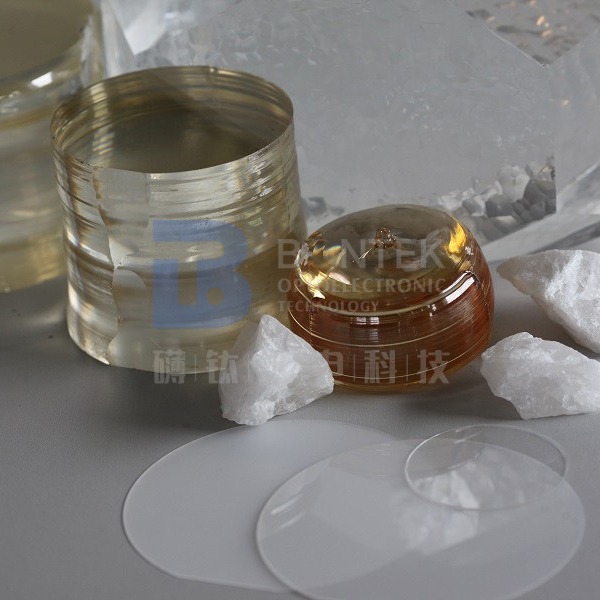
Y-cut and X-cut Lithium Niobate Wafer for Superior SAW Device Performance
Lithium niobate wafers are revolutionizing the optical technology industry with their unique combination of optical, piezoelectric, and ferroelectric properties. These wafers, made from high-quality lithium niobate crystal, offer unparalleled performance in a wide range of applications.
Their exceptional optical transparency and refractive index make
lithium niobate wafers ideal for use in optical modulators,
waveguides, and filters. Additionally, their piezoelectric
properties enable efficient conversion of optical signals into
electrical signals, vital for high-speed optical communication
systems.
With their high thermal stability and chemical durability, lithium
niobate wafers maintain performance even in harsh environments,
making them suitable for a wide range of industrial and scientific
applications.
Upgrade your optical technology with lithium niobate wafers and
enjoy superior performance, efficiency, and reliability. This is
the new benchmark in optical technology—a step forward in the
evolution of light.
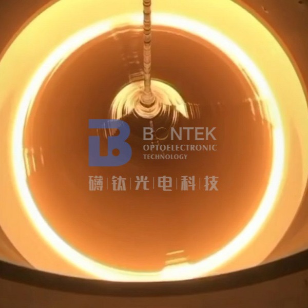
The development target of Lithium Niobate (LiNbO3) as the next generation SAW and optical material is always to produce larger diameter wafers to meet manufacturer’s requirements.

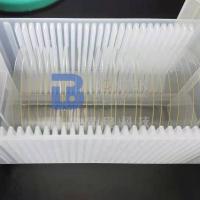
Material | 8" Lithium Niobate wafer |
Orientation | Z-cut or Y128°-cut |
Surface finish | Single or Double sides polish (DLP/SLP/ SSP/DSP all available ) |
Thickness | 0.35mm, 0.50mm, 1.00mm |
TTV | < 5µm |
BOW | ± 40um |
Warp | < 80µm |
Orientation flats | Semi Standard Notch |
Polished side Ra | Roughness Ra<10A |
Back Side Criteria | Roughness Ra:0.5-1.0µm GC#1000 |
Edge Rounding | Compliant with SEMI M1.2 Standard/refer to IEC62276 |
Crystal Sturucture | Trigonal, Space group R3c, Point group 3m |
Melting Point | 1253℃ |
Mohs Hardness | 5 |
Density | 4.64g/cm3 |
Deliquescence | None |
Optical Homogeneity | ~5x10⁻⁵/cm |
Transparency Range | 420-5200nm |
Absorption Coefficient | ~0.1%/cm @1064nm |


FAQs:
A: We look at ourselves as the piezo wafer specialist. We are the very first to work with Single Crystal Quartz in China about 30 years ago. Then gradually we step in the field of LiNbO3, LiTaO3, Quartz glass, LGS, CTGS etc. Especially, if you are looking for a piezo quartz supplier, we are the ultimate choice! We export millions of quartz blanks each year because we master the AT, SC and IT cuts with superior angle precision.
A: Yes, of course. We can fabricate as per your request. In addition, we are so experienced with piezo wafers that we can provide you relevant suggestions if you are not 100% sure about your choice. Besides, we do have some standard wafers in stock, please check with us.
A: Yes, we would suggest you go with the courier agent you are most familiar with (DHL, FedEX, UPS etc.). We can ship via your account. And, of course, we will pack the products safely in acceptable size to help you save the shipping cost. If you need us to take care of the freight, it’s also not a problem. We also have good discount with the international courier companies.
A: The wafer products are fragile and sometimes expensive. The last thing, as the manufacturer, we want to see is the products we make were damaged during courier. As a result, we will pack the wafers adequately and put them in a proper carton filled with buffer sponge. However, accidents are inevitable sometimes. So, please follow the “Acceptance check” steps shown in the drawings below. If the unwanted happened, we will either give the replenishment or refund if you follow the checking steps.
Acceptance Check


