

Active Member
|
[China]

Address: Room 704-3, 7 / F, Building 9, Yard 8, Development Road, Changping District, Beijing
Contact name:Marina

Beijing Haina Lean Technology Co., Ltd |
|
|
For no proper printed circuit boards without designing, PCB Prototype is the basic way for making the circuit boards.
Our experience to build PCB prototypes is just 24 hours.
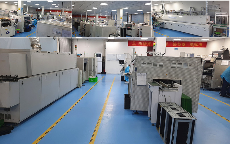
The prototype PCB assembly section of our manufacturing facility has a unique layout that allows for flexible use of both automated and manual parts-loading stations.
Our engineers is qualified and experienced in producing surface-mount (SMT), through-hole (THT) and mixed-technology components and fine-pitch parts and ball grid arrays (BGAs) for high-density FR-4 PCBs.
| FACTORY CAPABILITIES | |||
| No. | Items | 2019 | 2020 |
| 1 | HDI Capabilities | HDI ELIC (4+2+4) | HDI ELIC(5+2+5) |
| 2 | Max layer count | 32L | 36L |
| 3 | Board Thickness | Core thickness 0.05mm-1.5mm ,Fineshed board thickness 0.3-3.5mm | Core thickness 0.05mm-1.5mm ,Fineshed board thickness 0.3-3.5mm |
| 4 | Min.Hole Size | Laser 0.075mm Mechnical 0.15 | Laser 0.05mm Mechnical 0.15 |
| 5 | Min Line Width/Space | 0.035mm/0.035 | 0.030mm/0.030mm |
| 6 | Copper Thickness | 1/3oz-4oz | 1/3oz-6oz |
| 7 | Size Max Panel size | 700x610mm | 700x610mm |
| 8 | Registration Accuracy | +/-0.05mm | +/-0.05mm |
| 9 | Routing Accuracy | +/-0.075mm | +/-0.05mm |
| 10 | Min.BGA PAD | 0.15mm | 0.125mm |
| 11 | Max Aspect Ratio | 10:1 | 10:1 |
| 12 | Bow and Twist | 0.50% | 0.50% |
| 13 | Impedance Control Tolerance | +/-8% | +/-5% |
| 14 | Daily output | 3,000m2 (Max capacity of equipment) | 4,000m2 (Max capacity of equipment) |
| 15 | Surface Finishing | HASL Lead Free /ENEPING /ENIG /HASL /FINGER GOLD/IMMERSION TIN/SELECTIVE THICK GOLD | |
| 16 | Raw Material | FR-4/Normal Tg/High Tg/Low Dk/HF FR4/PTEE/PI | |
| PCBA Capability | |||
| Material Type | Item | Min | Max |
| PCB | Dimension (length,width,height.mm) | 50*40*0.38 | 600*400*4.2 |
| Material | FR-4,CEM-1,CEM-3,Aluminium-based board,Rogers,ceramic plate,FPC | ||
| Surface finish | HASL,OSP,Immersion gold,Flash Gold Finger | ||
| Components | Chip&IC | 1005 | 55mm |
| BGA Pitch | 0.3mm | - | |
| QFP Pitch | 0.3mm | - | |
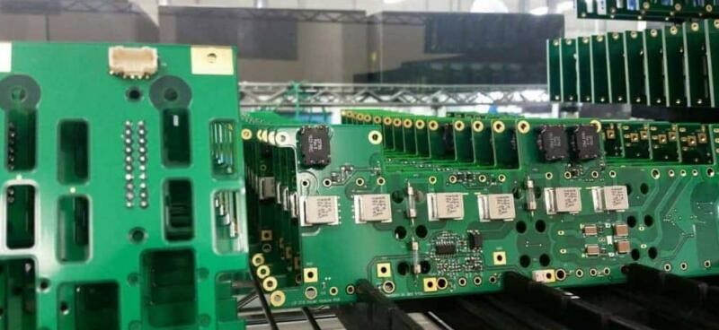
Our SMT capabilities:
SMT Assembly: SMT provides a flexible high technology. These solutions include:
7 high-speed placement machines,
7 automatic printers with fiducial alignment,
2 X-ray machines,
BGA maintenance machines,
ICT test machines
Our DIP function:
A-8 semi-assembly production line with four wave soldering machines
1 U-shaped automatic assembly line for box-type building products with test stations
High temperature / low temperature aging test furnace B-4 for products required for aging test
With time control and temperature control
All products are 100% inspected and tested during the DIP process
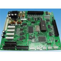
Haina lean Electronics Co.,Ltd is a competitive China customize pcba for medical breathing machine OEM manufacturer, supplier and vendor, you can get quick turn customize pcba for medical breathing machine production prototypes and samples from our factory.
Hot Tags: customize pcba for medical breathing machine, China, supplier, manufacturer, factory, OEM manufacturer, vendor, samples, production, prototypes, quick turn
PCB Assembly Prototype Process
1.Solder Paste stenciling---2.Surface Mount Technology (Pick and Place)---3.Reflow Soldering---4.Inspection and Quality Control---5.Through-Hole Component Insertion (DIP Process)---6.Final Inspection and Functional Test

| Product Type | Qty | Normal lead time | Quick-turn lead time |
| SMT+DIP | 1-50 | 1WD-2WD | 8H |
| SMT+DIP | 51-200 | 2WD-3WD | 1.5WD |
| SMT+DIP | 201-2000 | 3WD-4WD | 2WD |
| SMT+DIP | ≥2001 | 4WD-5WD | 3WD |
| PCBA(2-4Layer) | 1-50 | 2.5WD-3.5WD | 1WD |
| PCBA(2-4Layer) | 51-2000 | 5WD-6WD | 2.5WD |
| PCBA(2-4Layer) | ≥2001 | ≥7WD | 5WD |
| PCBA(6-10Layer) | 1-50 | 3WD-4WD | 2.5WD |
| PCBA(6-10Layer) | 51-2000 | 7WD-8WD | 6WD |
| PCBA(10-HDILayer) | 1-50 | 7WD-9WD | 5WD |
| PCBA(10-HDILayer) | 51-2000 | 9WD-11WD | 7WD |
Our products are widely used in communication equipment, industrial control, consumer electronics, medical equipment, aerospace, light-emitting diode lighting, automotive electronics.


PCB: Vacuum packaging with carton box
PCBA: ESD packaging with carton box


