

Active Member
|
[China]

Address: Room 704-3, 7 / F, Building 9, Yard 8, Development Road, Changping District, Beijing
Contact name:Marina

Beijing Haina Lean Technology Co., Ltd |

|
|
HF PCBs are regularly used for HDI technology. Also used extensively in high speed communications, telecommunications, and RF microwave technology. Satellite communication growing rapidly, information products move towards high speed and high frequency. Thus developing new products always need to use high frequency substrate, satellite system, mobile telephone receiving base station and so on, these communication products must use high frequency PCB.
In the next few years, information products will develop fastly, and high-frequency substrates will be in large demand.
The features of high frequency PCB as following:
1. DK should be small and stable enough, usually the smaller the better, high DK may lead to signal transmission delay.
2. DF should be small, which mainly affect quality of signal transmission, the smaller DF could make smaller signal wastage accordingly.
3. The thermal expansivity should be the same with copper foil as much as possible, because the difference will lead to copper foil separated in the changes of cold and heat.
4. Water absorptivity must be low, high water absorptivity will affect DK and DF when in the wet environment.
5. Heat resisting property, chemistry resisting, impact endurance, peel off resisting must be good.
Generally speaking, high frequency can be defined as frequency above 1GHz. Currently, polyfluortetraethylene(PTFE) material is widely used in high frequency PCB manufacturing, it's also called Teflon, which frequency is normally above 5GHz. In addition, FR4 or PPO substrate can be used to the product frequency among 1GHz~10GHz.
| FACTORY CAPABILITIES | |||
| No. | Items | 2019 | 2020 |
| 1 | HDI Capabilities | HDI ELIC (4+2+4) | HDI ELIC(5+2+5) |
| 2 | Max layer count | 32L | 36L |
| 3 | Board Thickness | Core thickness 0.05mm-1.5mm ,Fineshed board thickness 0.3-3.5mm | Core thickness 0.05mm-1.5mm ,Fineshed board thickness 0.3-3.5mm |
| 4 | Min.Hole Size | Laser 0.075mm | Laser 0.05mm |
| Mechnical 0.15mm | Mechnical 0.15mm | ||
| 5 | Min Line Width/Space | 0.035mm/0.035mm | 0.030mm/0.030mm |
| 6 | Copper Thickness | 1/3oz-4oz | 1/3oz-6oz |
| 7 | Size Max Panel size | 700x610mm | 700x610mm |
| 8 | Registration Accuracy | +/-0.05mm | +/-0.05mm |
| 9 | Routing Accuracy | +/-0.075mm | +/-0.05mm |
| 10 | Min.BGA PAD | 0.15mm | 0.125mm |
| 11 | Max Aspect Ratio | 10:1 | 10:1 |
| 12 | Bow and Twist | 0.50% | 0.50% |
| 13 | Impedance Control Tolerance | +/-8% | +/-5% |
| 14 | Daily Output | 3,000m2 (Max capacity of equipment) | 4,000m2 (Max capacity of equipment) |
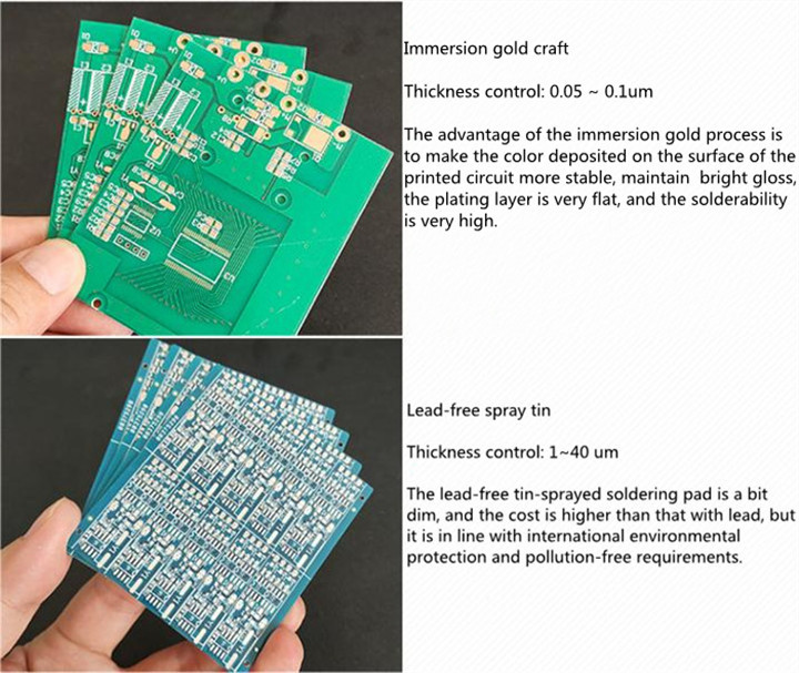
| 15 | Surface Finishing | ENEPING /ENIG /HASL /FINGER GOLD/IMMERSION TIN/SELECTIVE THICK GOLD | |
| 16 | Raw Material | FR-4/Normal Tg/High Tg/Low Dk/HF FR4/PTEE/PI | |
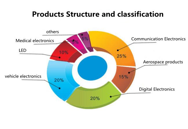
Market Success:
Products are mainly exported to Europe and USA;
Our customers spread over more than 80 countries;
Products are widely used in various industries.
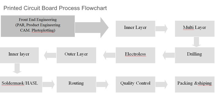
Multilayer PCB Craftsmanship
PCB Process
Wet process,Dry process
FOR MULTILAYER MANUFACTURE PROCESS:Laminate cut, scrubbing, Image
transfer, internal layer, Exposure, Developing, ETCHING, black /
brown oxygen, lay up, Laminating, Drilling, scrubbing, Plated
through hole, PTH panel plating, pattern plating (plated resist),
Etching, Inspection, Printing solder mask, Exposure, Developing,
Hot Cured, Hot Air Leveling, IMMERSION GOLD, Printing legend ink
(silkscreen printing), Hot Cured, Routing, punch, Bare board
testing, Final Inspection, Packing, Delivery
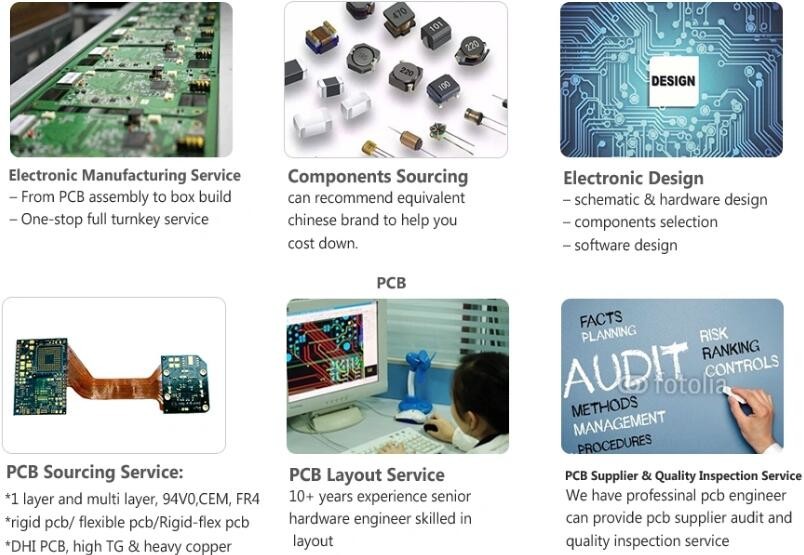
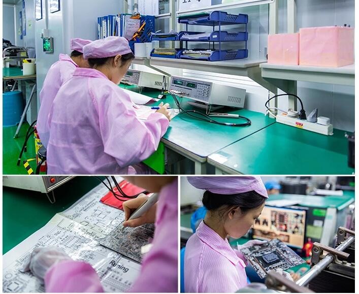
Electronic Manufacturing Service
PCB Electronic Design
PCB Layout Service
PCB Supplier & Quality Inspection Service
PCBA Components Sourcing
PCB Assembly process service
| Prototype PCB | Batch | Prototype | Expedited |
| Double sides | 9 Days | 5 Days | 45h |
| Four-layer | 10 Days | 5 Days | 3 Days |
| Six-layer | 12 Days | 6 Days | 3 Days |
| Eight-layer | 12 Days | 7 Days | 4 Days |
| Ten-layer | 14 Days | 10 Days | 4Days |
| Twelve-layer | 14 Days | 10 Days | 5 Days |
| Fourteen-layer | 16 Days | 12Days | 6 Days |
| Sixteen-layer | 16 Days | 12 Days | 6 Days |
| Eighteen-layer | 18 Days | 14 Days | 6 Days |
| Twenty-layer | 18 Days | 14 Days | 10 Days |
| Twenty two-layer | 20 Days | 14 Days | 10 Days |
| Twenty four-layer | 20 Days | 14 Days | 10 Days |
| Twenty six-layer | 20 Days | 14 Days | 10 Days |
| Twenty eight-layer | 20 Days | 14 Days | 10 Days |
High Frequency PCB Application Field
Such as communication equipment, automotive electronics,
instrumentation, global positioning system, computer, MP4, power
supply, home appliances, etc.
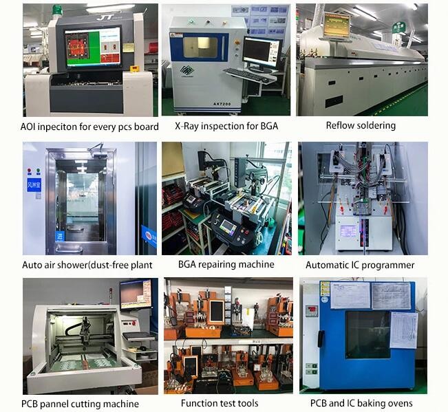

Testing service
1. Manual visual inspection of PCB board
2. PCB board online test
3. PCB board function test
4. AOI (Automatic optical inspection)
5. Automatic X-ray inspection
6. Laser detection system
7. Size detection
Above is the PCB testing service.
Haina lean Electronics provides custom test service according
to client's requirements and products.
Usually Haina lean Electronics Co.,Ltd PCBA Tech offers a full
range of testing service. Including:
1. AOI(Automatic Optical Inspection)
2. Function Testing
3. In Circuit Testing
4. Testing Jig
5. Testing Service
6. X-Ray for BGA Testing
7. Printing Solder Paste Test
Each board is carefully examined by our dedicated inspection team
using AOI and high magnification viewers.
Using our X-Ray machine, we test PCBs to component level and all
wiring is fully inspected and tested.
Flash testing and earth bonding tests can also be undertaken where
required.
PCB: Vacuum packaging with carton box
PCBA: ESD packaging with carton box

FAQ
Q1.
What's your MOQ ?
No Moq ,We accept small orders as well as mass production.
Q2.
For small quantity orders, can you produce prototype PCB?
Haina lean Electronics Co., has the capability to produce circuit
boards in any amount.
Q3.
Can You provide fast rotating PCB ?
Yes , we can provide fast service 24 hours .
Q4.
What are the services you can provide ?
One-stop contract manufacturing
PCB board, PCB Design & Layout, PCB Assembly, PCBA
programming & functional testing, Electronic components
purchasing service,
Enclosure molding & final assembly with
labels,instructions,enclosure, boxes.
Q5.
Whether all PCBA s will be tested before delivery ?
Yes , we will test each piece of PCBA product under your testing
methods ,to ensure quality and functionality .
Q6.
Do you provide OEM service ?
Yes ,we offer PCB and PCBA OEM Service , we manufacture the PCB and
PCBA products to your design and requirements .
Q7.
Shipping Cost ?
The shipping cost is determined by the destination ,weight ,packing
size of the goods .We can provide shipping, air, land, express and
other transportation services .
Q8.
Do you accept process materials supplied by clients?
Yes, we can provide component source, and we also accept component
from client. OEM and ODM orders are accepted.


