

Active Member
|
[China]

Address: Room 704-3, 7 / F, Building 9, Yard 8, Development Road, Changping District, Beijing
Contact name:Marina

Beijing Haina Lean Technology Co., Ltd |
|
|
HDI PCB, also known as high-density interconnect PCB, is a kind of PCB with a higher wiring density per unit area than traditional boards. HDI boards are more compact and have smaller vias, pads, copper traces and spaces. As a result, HDIs have denser wiring resulting in lighter weight, more compact, lower layer count PCBs. HDI PCB is more fit into the little spaces and have a smaller amount of mass than conservative PCB designs.
| Item | Capabilities |
| Number of Layers | 1 - 36layers |
| Order Quantity | 1pc - 10000+pcs |
| Material | FR4 standard Tg 140°C,FR4 High Tg 170°C, FR4 and Rogers combined lamination |
| Board Size | 700*610mm |
| Board Thickness | 0.3mm - 3.5mm |
| Copper Weight (Finished) | 0.33oz - 6.0oz |
| Min Tracing/Spacing | 3mil |
| Solder Mask Sides | As per the file |
| Solder Mask Color | Green, White, Blue, Black, Red, Yellow |
| Silkscreen Sides | As per the file |
| Silkscreen Color | White, Black, Yellow ,Etc |
| Surface Finish | HASL - Hot Air Solder Leveling |
| Lead Free HASL - RoHS | |
| ENIG - Electroless Nickle/Immersion Gold - RoHS | |
| Immersion Silver - RoHS | |
| Immersion Tin - RoHS | |
| OSP - Organic Solderability Preservatives - RoHS | |
| Min Annular Ring | 4mil, 3mil - laser drill |
| Min Drilling Hole Diameter | 6mil, 4mil - laser drill |
| HDI Capabilities | HDI ELIC (5+2+5) |
| Other Techniques | Flex-rigid combination |
| Via In Pad | |
| Buried Capacitor (only for Prototype PCB total area ≤1m²) |
1.through vias from surface to surface,
2.with buried vias and through vias,
3.two or more HDI layer with through vias,
4.passive substrate with no electrical connection,
5.coreless construction using layer pairs
6.alternate constructions of coreless constructions using layer
pairs.

Board Cut - Inner Wet film -DES - AOI - Brown Oxido - Outer Layer Press - Out Layer Lamination - X-RAY & Rounting - Copper reduce & brown oxide - Laser Drilling - Drilling - Desmear PTH - Panel plating - Outer Layer dry film - Etching - AOI- Impedance Testing - S/M Pluged hole - Solder Mask - Component Mark - Impedance testing - Immersion Gold -V-cut - Routing - Electrical Test - FQC - FQA -Package -Shipment

PCB design:
we can provide circuit design & PCB layout support.
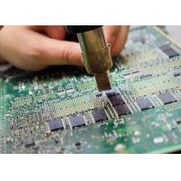
SMT Assembly:
Leading edge surface mount population technologies.
PTH Assembly:
RoHS compliant wave soldering & hand soldering capabilities.
PCB Fabrication:
You only need provide Gerber files or other design files .
Component procurement:
we have rich experience purchasing & material control expertise
team.
Product Assembly:
Complete turnkey solutions
Function Test & Inspection:
We offer test & inspection services on PCB & Assembly
(X-ray,ICT, AOI and Functional tests)


1.High Component Density
2.Space-saving
3.Lightweight Boards
4.Fast Processing
5.Save Number of Layers
6.Accommodate Low Pitch Packages
7.High Reliability
Automotive and aerospace industries, where lower weight can mean more efficient operation, have been utilizing HDI PCBs at an increasing rate. such as onboard WiFi and GPS, rearview cameras and backup sensors rely on HDI PCBs. As automotive technology continues to advance, HDI tech will likely play an increasingly important role.
HDI PCBs are also prominently featured in medical devices; advanced electronic medical devices such as equipment for monitoring, imaging, surgical procedures, laboratory analysis etc., and incorporate HDI boards. The high-density technology promotes improved performance and smaller, more cost-effective devices, potentially improving the accuracy of monitoring and medical testing.
Industrial automation requires abundant computerization, and IoT devices are becoming more common in manufacturing, warehousing, and other industrial settings. Many of these advanced equipment employ HDI technology. Today, businesses use electronic tools to keep track of inventory and monitor equipment performance. Increasingly, machinery includes smart sensors that collect usage data and connect to the internet to communicate with other smart devices, as well as to relay information to management and help optimize operations.
Except mentioned above, you'll also can find high-density interconnect PCBs in all types of digital devices, like smartphones and tablets, in automobiles, aircraft , mobile /cellular phones, touch-screen devices, laptop computers, digital cameras, 4/5G network communications, and military applications such as avionics and smart munitions.
| Product Type | Qty | Normal lead time | Quick-turn lead time |
| SMT+DIP | 1-50 | 1WD-2WD | 8H |
| SMT+DIP | 51-200 | 2WD-3WD | 1.5WD |
| SMT+DIP | 201-2000 | 3WD-4WD | 2WD |
| SMT+DIP | ≥2001 | 4WD-5WD | 3WD |
| PCBA(2-4Layer) | 1-50 | 2.5WD-3.5WD | 1WD |
| PCBA(2-4Layer) | 51-2000 | 5WD-6WD | 2.5WD |
| PCBA(2-4Layer) | ≥2001 | ≥7WD | 5WD |
| PCBA(6-10Layer) | 1-50 | 3WD-4WD | 2.5WD |
| PCBA(6-10Layer) | 51-2000 | 7WD-8WD | 6WD |
| PCBA(10-HDILayer) | 1-50 | 7WD-9WD | 5WD |
| PCBA(10-HDILayer) | 51-2000 | 9WD-11WD | 7WD |

PCB: Vacuum packaging with carton box
PCBA: ESD packaging with carton box

Q1:What kind of PCB file format can you accept for production?
Gerber, PROTEL 99SE, PROTEL DXP, CAM350, ODB+(.TGZ)
Q2:Is my PCB files safe when I submit them to you for manufacturing?
We respect customer's copyright and will never manufacture PCB for someone else with your files unless we receive written permission from you, nor we'll share these files with any other 3rd parties.
Q3:What payments do you accept ?
-Telex Transfer(T/T),Western Union,Letter of Credit(L/C)
-Paypal,AliPay,Credit Card
Q4:How to get the PCB?
A:For small packages, we will ship the boards to you by
DHL,UPS,FedEx,EMS. Door to door service! You will get your PCBs at
your home.
B:For heavy goods more than 300kg, we may ship your boards by ship
or by air to save freight cost. Of course, if you have your own
forwarder, we may contact them for dealing with your shipment.
Q5:What is your minimum order quantity?
Our MOQ is 1 PCS.
Q6: Can we visit your company?
No problem. You are welcome to visit us in Beijing. Or the branch factory is in Tianjin.
Q7: How can you ensure the quality of the PCB?
Our PCBs are 100% test including Flying Probe Test, E-test and AOI.
Haina lean Electronics Co., Ltd is a one-stop EMS supplier integrating PCB design, PCB manufacturing, Component sourcing and PCB assembly.
Our company was established in May 1, 2012 in Beijing. And expansion was completed in June 2016. The company is specialized in electronic products supporting processing services, mainly to undertake circuit board design, layout production, components procurement, PCB plate making, circuit board welding assembly debugging and other OEM/ODM services.
Our first factory is located in Changping District, Beijing, the main radiation Haidian, Changping, Chaoyang three areas of Beijing. Since our company’s establishment, we have been adhering to creating high quality, high efficiency, low-cost business philosophy based on the circuit board processing industry for customers. Most of the key staff of the company are mature technical talents who have been engaged in the industry for more than 10 years, and have rich experience in the production of SMT and DIP, also has rich experience in production for high density & difficulty to package components such as BGA. The factory covers an area of 1500 square meters. Since its establishment, we obtain a good reputation in the industry through the continuous efforts of all staff and high quality service . Our second branch plant is located in Langfang city, and mainly cover Fengtai and Daxing Yizhuang area.
The company pursues "inclusiveness, excellence, people-oriented". Constantly innovate, take technology as the core, regard quality as life, and wholeheartedly provide customers with high-quality and high-efficiency humanized services.We are willing to serve our customers with the principle of continuous honesty & trustworthiness, pragmatism and innovation.
At present, the main cooperation industries are automotive electronics, communications, audio and video, optoelectronics, robotics, hydroelectric power, medical care, aerospace, education, radio frequency, power supply, printer etc industries.


