

Active Member
|
[China]

Address: Room 704-3, 7 / F, Building 9, Yard 8, Development Road, Changping District, Beijing
Contact name:Marina

Beijing Haina Lean Technology Co., Ltd |

|
|
Here at Haina lean Electronics Co., Ltd, Standard PCB service refers to full feature printed circuit board manufacturing service. With 10+ years' experience in PCB fabrication, we have handled hundreds of thousands of PCB projects, and covered almost all kinds of substrate materials including FR4, Aluminum, Rogers, etc.
A bare board PCB (printed circuit board) and the bare board testing play critical roles in PCB creation. Bare board, is the PCB before the electric components or through holes are placed on it. A bare board comprise: Substrate; Metal Coating; Conductive Pathways.
Through a bare board layout, you could determine the placement of the components. In addition, the bare board testing can go a long way in ensuring that what you have is a reliable product.
We can configure PCB bare boards as per your specifications while also offering effective bare PCB testing capabilities. Our factory is a leading bare board provider in China. We can manufacture configurations of bare circuit boards based on your custom specification.
Our bare printed circuit board also assist you in penalization, place your PCB on large boards, mounting and plating process. We understand the complexity of PCB bare board manufacturing. Our goal is to provide best product which can fit your needs and best customer service.
Our factory is the first class manufacturer of HDI PCB , and undertake various board PCB services, including 1-36, HDI, thick copper layer, rigid flex, high frequency, Rogers+FR-4 mixed medium volume, lamination, buried aluminum, copper substrate, plate making proofing or quick expedited PCB proofing.
PCB Boards include Single-layer, Double-layer, Multi-layer, Rigid Board, Rigid-flexible Board, Flexible Board, High Frequency Board,
HDI PCB board, Aluminum Substrate etc.
Product Description:
Layers: 1-36
Base
material: FR4 CEM-1
Thickness: 0.2-5.0mm
Solder mask: Green, black, red, yellow, white
Min. Line width: 0.03mm
Min. Line space: 0.03mm
Min. Hole diameter: Laser 0.05mm,mechnical 0.1mm
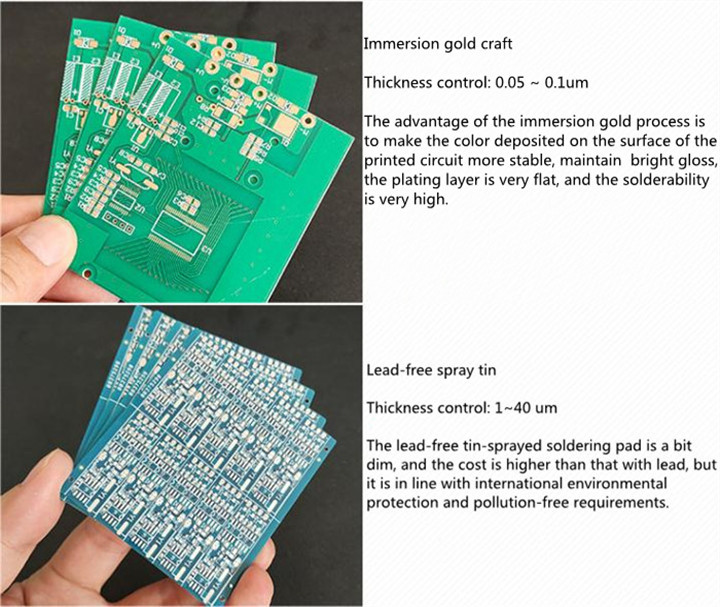
Surface treatment: Immersion gold, OSP. Lead free HASL.
Blind/buried via holes: OK
lead time: Seven to ten days (HDI: About 30 days)
Single to double sides pcb delivery time: 12-24 hours
4-layer to 8-layer pcb delivery time: 48-96 hours
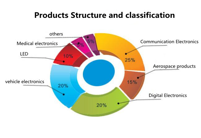
Market Success:
Products are mainly exported to Europe and USA;
Our customers spread over more than 80 countries;
Products are widely used in various industries.
Our factory' services:
high quality bare PCB, prototype PCB, PCB layout, PCB design service, PCB assembly service, components sourcing, function test,conformal coating and complete assembly for partners.
| FACTORY CAPABILITIES | |||
| No. | Items | 2019 | 2020 |
| 1 | HDI Capabilities | HDI ELIC (4+2+4) | HDI ELIC(5+2+5) |
| 2 | Max layer count | 32L | 36L |
| 3 | Board Thickness | Core thickness 0.05mm-1.5mm ,Fineshed board thickness 0.3-3.5mm | Core thickness 0.05mm-1.5mm ,Fineshed board thickness 0.3-3.5mm |
| 4 | Min.Hole Size | Laser 0.075mm | Laser 0.05mm |
| Mechnical 0.15mm | Mechnical 0.15mm | ||
| 5 | Min Line Width/Space | 0.035mm/0.035mm | 0.030mm/0.030mm |
| 6 | Copper Thickness | 1/3oz-4oz | 1/3oz-6oz |
| 7 | Size Max Panel size | 700x610mm | 700x610mm |
| 8 | Registration Accuracy | +/-0.05mm | +/-0.05mm |
| 9 | Routing Accuracy | +/-0.075mm | +/-0.05mm |
| 10 | Min.BGA PAD | 0.15mm | 0.125mm |
| 11 | Max Aspect Ratio | 10:1 | 10:1 |
| 12 | Bow and Twist | 0.50% | 0.50% |
| 13 | Impedance Control Tolerance | +/-8% | +/-5% |
| 14 | Daily Output | 3,000m2 (Max capacity of equipment) | 4,000m2 (Max capacity of equipment) |
| 15 | Surface Finishing | ENEPING /ENIG /HASL /FINGER GOLD/IMMERSION TIN/SELECTIVE THICK GOLD | |
| 16 | Raw Material | FR-4/Normal Tg/High Tg/Low Dk/HF FR4/PTEE/PI | |
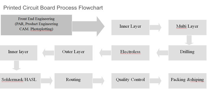
PCB Process
Wet process,Dry process
FOR MULTILAYER MANUFACTURE PROCESS:Laminate cut, scrubbing, Image
transfer, internal layer, Exposure, Developing, ETCHING, black /
brown oxygen, lay up, Laminating, Drilling, scrubbing, Plated
through hole, PTH panel plating, pattern plating (plated resist),
Etching, Inspection, Printing solder mask, Exposure, Developing,
Hot Cured, Hot Air Leveling, IMMERSION GOLD, Printing legend ink
(silkscreen printing), Hot Cured, Routing, punch, Bare board
testing, Final Inspection, Packing, Delivery

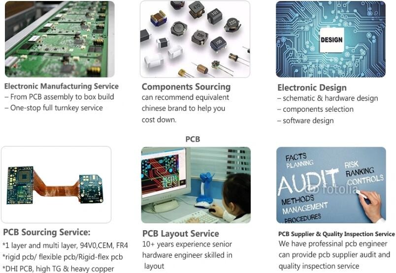
Our service
Electronic Manufacturing Service
PCB Electronic Design
PCB Layout Service
PCB Supplier & Quality Inspection Service
PCBA Components Sourcing
PCB Assembly process service
| Prototype PCB | Batch | Prototype | Expedited |
| Double sides | 9 Days | 5 Days | 45h |
| Four-layer | 10 Days | 5 Days | 3 Days |
| Six-layer | 12 Days | 6 Days | 3 Days |
| Eight-layer | 12 Days | 7 Days | 4 Days |
| Ten-layer | 14 Days | 10 Days | 4Days |
| Twelve-layer | 14 Days | 10 Days | 5 Days |
| Fourteen-layer | 16 Days | 12Days | 6 Days |
| Sixteen-layer | 16 Days | 12 Days | 6 Days |
| Eighteen-layer | 18 Days | 14 Days | 6 Days |
| Twenty-layer | 18 Days | 14 Days | 10 Days |
| Twenty two-layer | 20 Days | 14 Days | 10 Days |
| Twenty four-layer | 20 Days | 14 Days | 10 Days |
| Twenty six-layer | 20 Days | 14 Days | 10 Days |
| Twenty eight-layer | 20 Days | 14 Days | 10 Days |
Multilayer PCB Application Field
Printed circuit boards and PCB Assembly are widey used in many
communication industry, power, security, optoelectronics,
industrial control, medical equipments, consumer electronics and
automobile industry etc field.

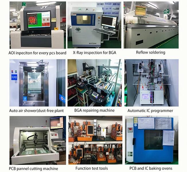

Testing service
1. Manual visual inspection of PCB board
2. PCB board online test
3. PCB board function test
4. AOI (Automatic optical inspection)
5. Automatic X-ray inspection
6. Laser detection system
7. Size detection
Above is the PCB testing service.
Haina lean Electronics provides custom test service according
to client's requirements and products.
Usually Haina lean Electronics Co.,Ltd PCBA Tech offers a full
range of testing service. Including:
1. AOI(Automatic Optical Inspection)
2. Function Testing
3. In Circuit Testing
4. Testing Jig
5. Testing Service
6. X-Ray for BGA Testing
7. Printing Solder Paste Test
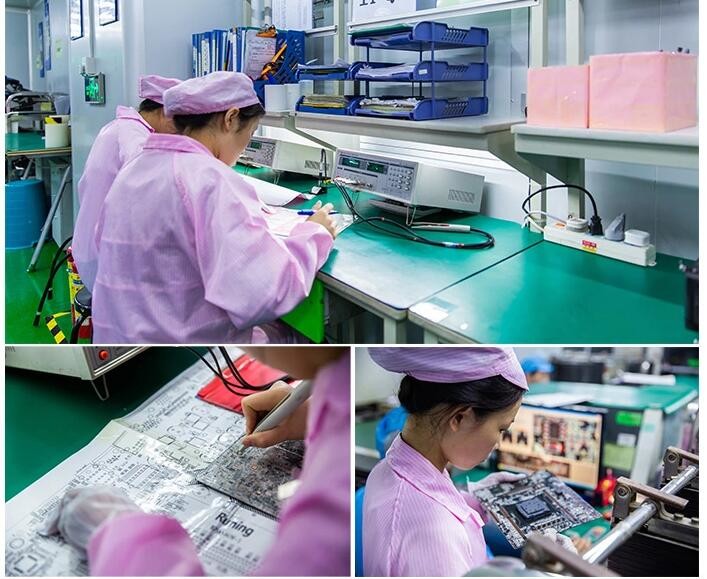
Each board is carefully examined by our dedicated inspection team
using AOI and high magnification viewers.
Using our X-Ray machine, we test PCBs to component level and all
wiring is fully inspected and tested.
Flash testing and earth bonding tests can also be undertaken where
required.
Partners

PCB: Vacuum packaging with carton box
PCBA: ESD packaging with carton box

Why choose us?
Welcome to visit our factory, Haina lean Electronics Co., Ltd.
1. Experienced: Focus on PCB And PCBA munufacturing over 10 years.
2. Professional: Expertise engineer with barrier-free English
3. Rapid delivery: On-time delivery rate reaches 98%
4.Cost effective: No excessive profits. Lower cost with same
quality And service
FAQ
Q1.
What's your MOQ ?
No Moq ,We accept small orders as well as mass production.
Q2.
For small quantity orders, can you produce prototype PCB?
Haina lean Electronics Co., has the capability to produce circuit
boards in any amount.
Q3.
Can You provide fast rotating PCB ?
Yes , we can provide fast service 24 hours .
Q4.
What are the services you can provide ?
One-stop contract manufacturing
PCB board, PCB Design & Layout, PCB Assembly, PCBA
programming & functional testing, Electronic components
purchasing service,
Enclosure molding & final assembly with
labels,instructions,enclosure, boxes.
Q5.
Whether all PCBA s will be tested before delivery ?
Yes , we will test each piece of PCBA product under your testing
methods ,to ensure quality and functionality .
Q6.
Do you provide OEM service ?
Yes ,we offer PCB and PCBA OEM Service , we manufacture the PCB and
PCBA products to your design and requirements .
Q7.
Shipping Cost ?
The shipping cost is determined by the destination ,weight ,packing
size of the goods .We can provide shipping, air, land, express and
other transportation services .
Q8.
Do you accept process materials supplied by clients?
Yes, we can provide component source, and we also accept component
from client. OEM and ODM orders are accepted.
Company Information
Haina lean Electronics Co., Ltd is a one-stop EMS supplier
integrating PCB design, PCB manufacturing, Component sourcing and
PCB assembly.
Our company was established in May 1, 2012 in Beijing. And
expansion was completed in June 2016. The company is specialized in
electronic products supporting processing services, mainly to
undertake circuit board design, layout production, components
procurement, PCB plate making, circuit board welding assembly
debugging and other OEM/ODM services.
Our first factory is located in Changping District, Beijing, the
main radiation Haidian, Changping, Chaoyang three areas of Beijing.
Since our company’s establishment, we have been adhering to
creating high quality, high efficiency, low-cost business
philosophy based on the circuit board processing industry for
customers. Most of the key staff of the company are mature
technical talents who have been engaged in the industry for more
than 10 years, and have rich experience in the production of SMT
and DIP, also has rich experience in production for high density
& difficulty to package components such as BGA. The factory
covers an area of 1500 square meters. Since its establishment, we
obtain a good reputation in the industry through the continuous
efforts of all staff and high quality service . Our second branch
plant is located in Langfang city, and mainly cover Fengtai and
Daxing Yizhuang area.
The company pursues "inclusiveness, excellence, people-oriented".
Constantly innovate, take technology as the core, regard quality as
life, and wholeheartedly provide customers with high-quality and
high-efficiency humanized services.We are willing to serve our
customers with the principle of continuous honesty &
trustworthiness, pragmatism and innovation.
Our customers are from over more than 80 countries. At present, the
main cooperation industries are automotive electronics,
communications, audio and video, optoelectronics, robotics,
hydroelectric power, medical care, aerospace, education, radio
frequency, power supply, printer etc industries.


