Home Companies Guangzhou Kaijin Precision Manufaturing Co., Ltd.

FR4 Customized PCB Prototype Service Manufacturer With HASL Surface Finish

Guangzhou Kaijin Precision Manufaturing Co., Ltd.

Contact Us

[China] country

Trade Verify

Contact name:Rain Kong

Inquir Now

Guangzhou Kaijin Precision Manufaturing Co., Ltd.

Verified Suppliers
  • Trust
    Seal
  • Verified
    Supplier
  • Credit
    Check
  • Capability
    Assessment

FR4 Customized PCB Prototype Service Manufacturer With HASL Surface Finish

Country/Region china
City & Province guangzhou
Categories Tool Processing Services
InquireNow

Product Details

FR4 PCB Prototype with HASL Surface Finish

Product Description:

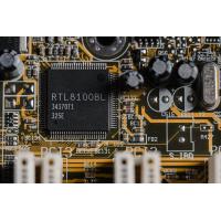
PCB Prototype is a type of printed circuit board (PCB) that is designed and manufactured with two layers of copper foil and a FR-4 base material. It is ideal for use in applications where the circuit must be flexible, such as medical and automotive electronics. The PCB Prototype features a minimum hole size of 0.2mm, copper thickness of 1oz, and a surface finish of HASL. Additionally, it has a minimum trace width of 0.2mm and a minimum space of 0.2mm, making it suitable for tightly packed and complex printed circuit boards. The FR4 double sided PCB is durable and reliable, providing a great solution for high-volume production and quick turnaround for prototype projects. It also offers a cost-effective option for PCB assembly.


Features:

  • Product Name: PCB Prototype
  • PCB QC: Flying Probe Test, E-test
  • Min Trace Width: 0.2mm
  • Copper Thickness: 1oz
  • PCBA QC: X-ray, AOI Test, Functional Test
  • Surface Finish: HASL
  • PCB Board Making: Yes
  • Prototype Circuit Board: Yes
  • Low Cost PCB Prototype: Yes
 

Technical Parameters:

PropertyValue
SilkscreenWhite
Surface FinishHASL
Copper Thickness1oz
PCBA QCX-ray,AOI Test,Functional Test
Board Thickness1.6mm
Impedance ControlYes
Solder MaskGreen
Layer2
Min Space0.2mm
Delivery Time3-5 Days
 

Applications:

PCB Prototype is a great solution for a wide range of applications, from prototyping to production. It's built with FR4 double sided PCB, with an overall layer of 2. It features a white silkscreen, a green solder mask, and a HASL surface finish. The delivery time is usually within 3-5 days. This type of PCB is perfect for prototyping, as it's made with flexible material. With its reliable performance and quick delivery, PCB Prototype is the go-to choice for many engineers and designers.


Customization:

Customized PCB Prototype Service
  • 4 layer pcb prototype
  • Prototype circuit board
  • Silkscreen: White
  • Copper Thickness: 1oz
  • Min Annular Ring: 0.1mm
  • Min Trace Width: 0.2mm
  • Delivery Time: 3-5 Days
 

Support and Services:

PCB Prototype offers technical support and services to ensure that your product is manufactured to the highest standards. Our technical support team is available to answer questions, provide advice, and troubleshoot any issues you may have with the prototype. Additionally, our services include prototyping, testing, and production of the final product.


Packing and Shipping:

Packaging and Shipping for PCB Prototype

The PCB Prototype product is packaged and shipped using a reliable and trusted courier service. The product is shipped in a well-protected box or package and is carefully monitored throughout the delivery process. All packaging materials meet the necessary safety and quality requirements.

The PCB Prototype product is shipped with a tracking number so it can be tracked at all times. All shipments are insured to ensure full coverage in the event of any damages or loss. The product is shipped with a detailed packing slip providing a list of all items included in the package.


FAQ:

PCB Prototype FAQs
Q1: What is PCB Prototype?
A1: PCB Prototype is a printed circuit board product that is used to test and verify the design of an electronic circuit. It is typically used in the early stages of product development before mass production.
Q2: What are the materials used to make PCB Prototype?
A2: PCB Prototype typically use materials such as copper, silicon, and other materials in the production process. Depending on the specific application, other materials may be used.
Q3: What are the advantages of using PCB Prototype?
A3: PCB Prototype provides designers with a low-cost, rapid prototyping solution to quickly test and verify the design of an electronic circuit. Additionally, it allows designers to make corrections and improvements to the design before committing to a large-scale production run.
Q4: Can PCB Prototype be customized?
A4: Yes, PCB Prototype can be customized to meet the specific needs of a customer’s application. This includes customizing the size, shape, and components of the board.
Q5: What is the lead time for PCB Prototype?
A5: The lead time for PCB Prototype depends on the complexity of the design and the specific components used. Generally, lead times range from a few days to a few weeks.

Hot Products

FR4 PCB Prototype with HASL Surface Finish and Green SolderMask Product Description: PCB Prototype ...
Custom 2-Layer PCB Board with Min Hole Size 0.2mm and Green Solder Mask Product Description: PCB ...
4 Layer PCB Prototype with Min Hole Size 0.2mm FR4 Material Product Description: PCB Prototype PCB ...
FR4 Double Sided PCB 0.1mm Min Annular Ring 2 Layer Product Description: PCB Prototype is a double...
FR4 PCB Prototype with HASL Surface Finish Product Description: PCB Prototype is a type of printed ...
PCB QC E-Test AOI Inspection Delivered In 3-5 Days Product Description: PCB Prototype PCB Prototype ...