
|
|
[China]

Trade Verify
Address: Corporate Drive, Irvine, California, USA
Contact name:

LT CIRCUIT CO.,LTD. |
|
Verified Suppliers
|
|
|
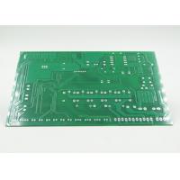
Medical Instruments Heavy Copper PCB IPC II Standard 100% Test
Our Print Circuit Board (PCB) is a robust foundation for any demanding electrical application, particularly suited for medical instruments where reliability and precision are crucial. This two-layered PCB ensures that your medical devices perform consistently and accurately, helping medical professionals provide exceptional patient care. With an impressive minimum line width of just 3mil (0.075mm), our PCB provides the fine detail needed for complex circuit designs without compromising on power or signal integrity.
The Heavy Copper PCB product is not just a standard circuit board; it's a durable platform designed for enhanced current-carrying capacity and superior thermal management. Copper, known for its excellent electrical conductivity, is the main ingredient in our Copper-Rich PCB, ensuring minimal energy loss and optimal performance even in the most intricate medical devices. The thickness of the copper layer significantly exceeds that of conventional PCBs, making our Copper-Enriched PCB an ideal choice for high-power applications where typical boards might fail.
With a board size of 6*9cm, the Heavy Copper PCB is compact enough to fit into a variety of medical instruments while still providing ample space for necessary components and pathways. This size makes it an excellent choice for sophisticated medical applications where space is at a premium but performance cannot be compromised. Moreover, the Thick Copper PCB design allows for enduring reliability, which is vital for medical devices that often operate continuously and under critical conditions.
The use of thick copper in our PCB not only enhances the electrical performance but also contributes to mechanical strength. This is especially important in the medical field where equipment needs to withstand rigorous use and ensure uninterrupted operation. The robust nature of our Thick Copper PCB makes it resistant to thermal strains, physical stresses, and harsh chemicals commonly found in the medical environment. Moreover, the increased copper thickness allows for a larger cross-sectional area for current carrying, reducing the risk of circuit failure due to overheating.
Our advanced manufacturing techniques ensure that the minimum line width of 3mil is maintained throughout the PCB, allowing for a high-density layout that can accommodate more components without increasing the board size. This precision is crucial in medical instruments that require a multitude of functions within a compact form factor. The meticulous attention to detail in the design and production stages results in a Copper-Enriched PCB that not only meets but exceeds industry standards for performance and reliability.
In conclusion, the Heavy Copper PCB product combines the best in electrical engineering and materials science to provide a superior solution for medical instruments. The Copper-Rich PCB delivers exceptional electrical conductivity, thermal resistance, and structural integrity, making it the go-to choice for medical device manufacturers who demand the highest quality and dependability. The two-layer configuration of our Copper-Enriched PCB is meticulously designed to handle complex circuits with precision, paving the way for advancements in medical technology and patient care. Invest in a PCB that ensures your medical instruments operate flawlessly; choose our Heavy Copper PCB for excellence in every layer.
| Parameter | Specification |
|---|---|
| Hs Code | 8534009000 |
| Number Of Layers | 2 Layer |
| Minimum Line Space | 3mil (0.075mm) |
| Solder Mask | Blue |
| Standard | IPC-A-610 Class II-III |
| Application | Medical Instruments |
| Board Size | 6*9cm |
| Solder mask thickness | 20-50UM |
| Production Name | Print Circuit Board |
| Min Hole Size | 0.2MM |
The Heavy Copper PCB, defined by the Hs Code 8534009000, is an exceptional product designed for a broad range of applications and scenarios where enhanced power distribution, increased thermal management, and sturdy structural integrity are paramount. This Copper-Rich PCB, typically shipped in secure Carton + Binding Tape packaging to ensure its safe delivery, is a robust foundation for numerous high-demand electronic assemblies.
With a substantial composition that defines it as a High Copper Content PCB, this product is particularly suitable for power electronic devices that must withstand significant electrical loads and thermal stress. The 2 Layer configuration offers a balanced and compact design, making it ideal for space-constrained applications while still providing the necessary circuit complexity. The Minimum Line Width specification of 3mil (0.075mm) ensures high-density layouts can be achieved, allowing for intricate designs in power converters, power supply systems, and automotive electronics.
The Weighty Copper PCB is a perfect match for industrial controls where reliability and endurance are tested in harsh environments. The heavy copper tracks are capable of enduring extreme temperature variations and high current loads, which is essential for heavy machinery and equipment. Additionally, the aerospace industry, where reliability and maximum performance under stringent conditions are non-negotiable, finds excellent use of this type of PCB for its critical systems.
In the realm of consumer electronics, the High Copper Content PCB finds its use in high-performance computing and audio systems, where efficient heat dissipation and robust power delivery are necessary to maintain the integrity and longevity of the components. Furthermore, due to the 100% Testing protocol that each PCB undergoes, customers are assured of the highest quality and reliability for their sophisticated electronics.
Lastly, the Weighty Copper PCB's attributes are highly sought after in renewable energy applications, such as solar inverters and wind power generators, where the Copper-Rich PCB must handle high power outputs and provide long-term stability. This aligns with the growing demands for sustainable and reliable energy solutions. With its unique combination of heavy copper content, precise manufacturing, and comprehensive testing, the Heavy Copper PCB stands out as a critical component for a myriad of high-stakes electronic applications.
Product Name: Print Circuit Board
Production Customization Services: We specialize in manufacturing Thick Copper PCBs with advanced customization options to meet your specific needs. Our Copper-Enriched PCBs offer enhanced performance due to the increased copper content.
Solder Mask Thickness: Our Copper-Infused PCBs come with a solder mask thickness ranging from 20-50UM, ensuring robust protection and reliability.
Process: We utilize the Immersion Gold/Silver process for superior conductivity and to enhance the solderability of your heavy copper PCB.
Hs Code: 8534009000
Minimum Line Width: Precision engineering allows us to achieve a minimum line width of 3mil (0.075mm), suitable for complex and high-density circuit designs.
The Heavy Copper PCB product is supported by a comprehensive suite of technical support and services designed to ensure optimal performance and longevity. Our knowledgeable and experienced engineers are available to assist with any technical queries, from initial design to final implementation. We offer guidance on stack-up configuration, copper thickness, material selection, and thermal management to ensure your Heavy Copper PCB meets the highest standards.
We provide detailed documentation, including specifications, handling instructions, and best practices to help you get the most out of your Heavy Copper PCB. Our services include thermal analysis, signal integrity analysis, and power distribution network design, all tailored to support the specific requirements of Heavy Copper PCBs.
In case of any performance issues or faults, our technical team is prepared to provide troubleshooting assistance, fault diagnosis, and, when necessary, repair or replacement services. We are committed to delivering a quick and effective resolution to any product concerns, ensuring minimal downtime for your operations.
Our commitment to customer satisfaction extends beyond the sale, with ongoing support to help you adapt to evolving technical challenges and extend the life of your Heavy Copper PCB. We continually update our support resources to reflect the latest industry standards and technological advancements.


