
|
|
[China]

Trade Verify
Address: Corporate Drive, Irvine, California, USA
Contact name:

LT CIRCUIT CO.,LTD. |
|
Verified Suppliers
|
|
|
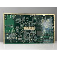
The HDI Any Layer PCBs (High-Density Integrated Circuit Interconnection Boards) represent the forefront of modern printed circuit board (PCB) technology, catering to the evolving need for smaller, more efficient, and highly integrated electronic components. Our state-of-the-art HDI PCBs offer unparalleled performance and reliability for a wide range of applications, including but not limited to, telecommunications, consumer electronics, automotive, and medical devices.
Our High-Density Interconnect (HDI) PCBs are manufactured with precision and the highest quality standards, ensuring that each board meets the rigorous demands of today's complex electronic circuits. With lead times ranging from a rapid 2-5 days, we are committed to delivering your HDI Any Layer PCBs quickly without compromising on quality, enabling you to speed up your product development cycle and go to market faster.
The surface finish of a PCB plays a critical role in its performance and longevity. Our HDI PCBs are available with a variety of surface finishes to meet the specific requirements of your application. Options include HASL (Hot Air Solder Leveling), ENIG (Electroless Nickel Immersion Gold), Immersion Silver, and OSP (Organic Solderability Preservatives). Each of these finishes offers unique benefits, such as excellent solderability, corrosion resistance, and wire bondability, ensuring that your HDI Any Layer PCB maintains its integrity throughout its operational life.
To ensure the highest quality of our High-Density Integrated Circuit Interconnection Boards, we employ advanced testing methods such as Flying Probe Test and E-test. These sophisticated testing protocols allow us to detect any potential issues early in the manufacturing process, thereby avoiding costly reworks or failures in the field. Testing is an integral part of our production process, which is why we invest heavily in state-of-the-art equipment and skilled technicians to perform comprehensive inspections on every HDI PCB we produce.
One of the most significant attributes of our HDI Any Layer PCBs is the minimum finished hole size of 0.1mm. This exceptional capability enables the creation of extremely fine features, which is essential for high-density interconnect designs where space is at a premium. The ability to accommodate such small vias allows for more complex and compact circuit designs, making it possible to achieve higher functionality in smaller form factors. This attribute is particularly beneficial for applications where space savings and increased performance are paramount.
The minimum hole size of 0.1mm is not only reflective of our technical capabilities but also of our commitment to innovation and the continuous pursuit of pushing the boundaries of PCB design. This feature facilitates the integration of multiple layers within the PCB, allowing for any-layer interconnections that can significantly enhance electrical performance and signal integrity. By leveraging the advanced capabilities of our HDI Any Layer PCBs, designers and engineers can realize their most ambitious projects with confidence.
In conclusion, our HDI Any Layer PCBs provide a robust and reliable interconnection solution for high-density integrated circuits. With rapid lead times, a range of surface finish options, rigorous testing protocols, and advanced design features such as a minimum finished hole size of 0.1mm, our products are designed to meet the challenges of today's electronic industry. Whether you are developing cutting-edge technology or optimizing existing designs, our High-Density Interconnect PCBs are the ideal choice for achieving high performance, reliability, and efficiency in your electronic products.
| Technical Parameter | Specification |
|---|---|
| Minimum Hole Size | 0.1mm |
| Min. Finished Hole Size | 0.1mm |
| Surface Finish | HASL, ENIG, Immersion Silver, OSP |
| Lead Time | 2-5 Days |
| Testing | Flying Probe Test, E-test |
| Silkscreen Color | White, Black, Yellow |
| Minimum Line Width/Spacing | 3mil/3mil |
| Layer Count | Any Layer |
| Copper Weight | 0.5oz-6oz |
| Thickness | 0.2mm-6.0mm |
The High Density Interconnect Any Layer (HDI Any Layer) PCBs are at the forefront of advanced circuit board technology, providing unparalleled flexibility and precision. With the capability to accommodate any layer count, these boards are designed to meet the rigorous demands of sophisticated electronic devices. The HDI Any Layer PCBs boast a minimum line width and spacing of just 3mil/3mil, making them ideal for applications where space is at a premium and high signal integrity is a must.
One of the primary application scenarios for the HDI Any Layer PCBs is in the realm of consumer electronics. These boards are perfect for smartphones, tablets, and laptops, where the high-density interconnect board technology allows for a greater number of functions in a smaller form factor. Additionally, wearable technology, which requires compact and efficient designs, benefits significantly from the any-layer interconnect board's ability to stack layers densely without compromising performance.
In the field of medical devices, the HDI Any Layer PCBs are crucial for ensuring that equipment such as handheld diagnostic devices and portable monitoring systems remain reliable and accurate. The fine line precision of these PCBs supports the high-speed signal transmission needed for critical medical technology, providing life-saving diagnostics and treatment in a miniaturized footprint.
Aerospace and defense systems also leverage the advanced capabilities of the HDI Any Layer PCBs. In these industries, the need for robust, high-performance boards that can withstand extreme conditions while maintaining a compact size is paramount. The HDI technology allows for complex multi-layer designs that are essential for navigation, communication, and surveillance systems.
The solder mask color options, including green, red, blue, black, yellow, and white, enable customization for specific design requirements and aesthetic preferences. This feature, combined with a rapid lead time of 2-5 days, ensures that projects can proceed quickly without compromising on quality. Moreover, the integrity of the HDI Any Layer PCBs is verified through rigorous testing methods such as Flying Probe Test and E-test, ensuring that each board meets the highest standards of functionality and reliability.
In summary, the HDI Any Layer PCBs are a versatile solution for a wide range of applications where density, precision, and reliability are crucial. Their adaptability to any layer count and their advanced manufacturing standards make them an essential component in cutting-edge electronic development across various industries.
Our HDI (High-Density Interconnect) Any Layer PCBs provide a sophisticated Multilayer Interconnect System with a range of customization options to meet your specific requirements. Our PCBs are ideal for applications that demand a Miniature Interconnect System and High-Density Assembly System, ensuring high performance and reliability.
Choose from a variety of silkscreen colors to match your design preferences or to help differentiate various PCBs in complex systems. We offer silkscreen colors in White, Black, and Yellow.
The HDI Any Layer PCBs are fabricated using high-quality FR-4 material, known for its excellent electrical insulation and mechanical stability, making it suitable for most applications.
To accommodate different design complexities and applications, our PCBs can be customized with a thickness ranging from 0.2mm to 6.0mm, providing flexibility in your product design.
Our precision manufacturing processes allow for a minimum annular ring of 3mil, ensuring reliable connections and adherence to stringent design specifications.
We understand the importance of time in product development, which is why we offer a fast lead time of 2-5 days, enabling you to accelerate your project timeline without compromising on quality.
Our HDI Any Layer PCBs are designed with the utmost precision and reliability in mind, ensuring high-density interconnect performance that meets the needs of today's sophisticated electronic applications. To provide you with the best support and ensure your success, we offer comprehensive technical support and services for our HDI Any Layer PCB products.
Technical Support:
Our dedicated team of experts is available to assist with any technical queries or issues you may encounter. From design challenges to questions about material specifications or manufacturing processes, we are here to provide guidance and solutions to ensure your PCBs perform as expected.
Design Review Services:
Before your PCB design goes into production, our engineers can conduct a thorough review to identify potential issues and suggest improvements. This proactive approach helps to minimize the risk of costly reworks and ensures that your PCBs are optimized for manufacturability and performance.
After-Sales Services:
We stand by the quality of our HDI Any Layer PCBs and are committed to your satisfaction. After your order is complete, we continue to provide support to address any concerns you may have with the product. Whether it's a question about installation or performance, our after-sales team is ready to assist you.
Quality Assurance:
Our HDI Any Layer PCBs undergo rigorous testing and quality control procedures to ensure they meet the highest industry standards. We are committed to delivering products that you can rely on for their performance and longevity.
Documentation and Resources:
Access a wealth of technical documentation, including datasheets, user manuals, and application notes, designed to provide you with detailed information on our HDI Any Layer PCBs. Our online resources are available to help you better understand and utilize our products.
For any assistance you require with our HDI Any Layer PCBs, please do not hesitate to reach out to our technical support team. We are here to ensure your experience with our products is seamless and successful.


