|
|
[China]

Trade Verify
Address: Address:Room624,Fangdichan development building,Guicheng south,Nanhai,Foshan,China
Contact name:Tracy

ONESEINE TECHNOLOGY CO.,LTD |
|
Verified Suppliers
|
|
|
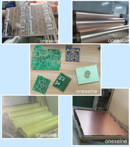
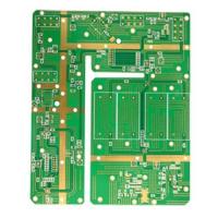
ISOLA PCB High TG Stable DK Value High Frequency Circuit Board
Quick detail:
Size: 18*10cm
Copper THK:35UM
Color: Green
Material: Isola laminate
Surface finish:Immersion gold,ENIG
6 layer 1.2mm thickness
Green solder mask,white silk screen
Line space and width:10mil
Certification:ISO9001/SGS/UL
Delivery time:3-7 working days
Most popular isola PCB material model:
Isola fr402,370HR,fr408,Isola410
Isola PCB |
Isola laminate |
Isola fr406 |
Isola 410 |
Isola 370HR |
Isola PCB laminate Advantage:
Have stock of Scarcity of isola 370HR material,
short time of incoming material,save costing for you
Isola substrate is a high performance 180°C glass transition temperature
(Tg) FR-4 system for multilayer Printed Wiring Board (PWB)
applications where maximum thermal performance and reliability
are required. 370HR laminate and prepreg products are
manufactured with a unique high performance multifunctional
epoxy resin, reinforced with electrical grade (E-glass) glass fabric.
This system provides improved thermal performance and low
expansion rates in comparison to traditional FR-4 while retaining
FR-4 processability.
In addition to this superior thermal performance, the mechanical,
chemical and moisture resistance properties all equal or exceed
the performance of traditional FR-4 materials. The 370HR system
is also laser fluorescing and UV blocking for maximum compatibility
with Automated Optical Inspection (AOI) systems, optical positioning
systems and photoimagable solder mask imaging.
370HR has proven to be best in class for sequential lamination
Isola PCB Features
• High Thermal Performance
Tg: 180°C (DSC)
Td: 360°C (TGA @ 5% wt loss)
• T260: 60 minutes
• T288: 15 minutes
• RoHS Compliant
• UV Blocking and AOI Fluorescence
High throughput and accuracy during PCB
fabrication and assembly
• Superior Processing
Closest to conventional FR-4 processing of all
high speed materials
• Core Material Standard Availability
Thickness: 0.002″ (0.05 mm) to 0.125″
(3.2 mm)
Available in full size sheet or panel form
• Prepreg Standard Availability
Roll or panel form
Tooling of prepreg panels available
• Copper Foil Type Availability
Standard HTE Grade 3
RTF (Reverse Treat Foil)
• Copper Weights
1 and 2 oz (18, 35 and 70 μm) available
Heavier copper available upon request
Thinner copper foil available upon request
• Glass Fabric Availability
Standard E-glass
Square weave glass fabric available
• Industry Approvals
IPC-4101D WAM1 /24 /121 /124
UL - File Number E41625
Qualified to UL's MCIL Program
High frequency PCB range:
Frequency Range: High-frequency PCBs are designed to operate in frequency ranges typically starting from a few megahertz (MHz) and extending into the gigahertz (GHz) and terahertz (THz) ranges. These PCBs are commonly used in applications such as wireless communication systems (e.g., cellular networks, Wi-Fi, Bluetooth), radar systems, satellite communication, and high-speed data transmission.
Signal Loss and Dispersion: At high frequencies, signal loss and dispersion become significant concerns. High-frequency PCBs employ techniques to minimize these effects, such as using low-loss dielectric materials, controlled impedance routing, and minimizing the length and number of vias.
PCB Stackup: The stackup configuration of a high-frequency PCB is carefully designed to address signal integrity requirements. It typically consists of multiple layers of copper traces, dielectric materials, and ground planes. The arrangement of these layers is optimized to control impedance, minimize crosstalk, and provide shielding.
RF Connectors: High-frequency PCBs often incorporate specialized RF connectors to ensure proper signal transmission and minimize losses. These connectors are designed to maintain consistent impedance and minimize reflections.
Electromagnetic Compatibility (EMC): High-frequency PCBs must comply with electromagnetic compatibility standards to prevent interference with other electronic devices and to avoid susceptibility to external interference. Proper grounding, shielding, and filtering techniques are employed to address EMC requirements.
Simulation and Analysis: Designing high-frequency PCBs often involves simulation and analysis using specialized software tools. These tools allow designers to assess signal integrity, impedance matching, and electromagnetic behavior before fabrication, helping to optimize the PCB design for high-frequency performance.
Fabrication Challenges: Fabricating high-frequency PCBs can be more challenging compared to standard PCBs. The use of specialized materials, controlled impedance requirements, and tight tolerances require advanced fabrication techniques such as accurate etching, controlled dielectric thickness, and precise drilling and plating processes.
Testing and Validation: High-frequency PCBs undergo rigorous testing and validation to ensure their performance meets the desired specifications. This includes impedance testing, signal integrity analysis, insertion loss measurement, and other RF and microwave tests.
It's important to note that the design and manufacturing of high-frequency PCBs are specialized areas requiring expertise in RF and microwave engineering, PCB layout, and fabrication processes. Working with experienced professionals and consulting relevant design guidelines and standards is crucial to ensure reliable performance at high frequencies.
High frequency PCB description:
High frequency PCB material in stock:
| Brand | Model | Thickness(mm) | DK(ER) |
| Rogers | RO4003C | 0.203mm,0.305mm,0.406mm,0.508mm,0.813mm,1.524mm | 3.38 ± 0.05 |
| RO4350B | 0.101mm,0.168mm,0.254mm,0.338mm,0.422mm,0.508mm,0.762mm,1.524mm | 3.48 ± 0.05 | |
| RO4360G2 | 0.203mm,0.305mm,0.406mm,0.508mm,0.610mm,0.813mm,1.524mm | 6.15 ± 0.15 | |
| RO4835 | 0.168mm,0.254mm,0.338mm,0.422mm,0.508mm,0.591mm, 0.676mm,0.762mm,1.524mm | 3.48 ± 0.05 | |
| RT5870 | 0.127mm,0.787mm,0.254mm,1.575mm,0.381mm,3.175mm,0.508mm | 2.33 2.33 ± 0.02 | |
| RT5880 | 0.127mm,0.787mm,0.254mm,1.575mm,0.381mm,3.175mm,0.508mm | 2.20 2.20 ± 0.02 | |
| RO3003 | 0.13mm,0.25mm,0.50mm,0.75mm,1.52mm | 3.00 ±0.04 | |
| RO3010 | 0.13mm,0.25mm,0.64mm,1.28mm | 10.2 ± 0.30 | |
| RO3006 | 0.13mm,0.25mm,0.64mm,1.28mm | 6.15 ± 0.15 | |
| RO3203 | 0.25mm,0.50mm,0.75mm,1.52mm | 3.02±0.04 | |
| RO3210 | 0.64mm,1.28mm | 10.2±0.50 | |
| RO3206 | 0.64mm,1.28mm | 6.15±0.15 | |
| R03035 | 0.13mm,0.25mm,0.50mm,0.75mm,1.52mm | 3.50 ± 0.05 | |
| RT6002 | 0.127mm,0.254mm,0.508mm,0.762mm,1.524mm,3.048mm | 2.94 ± 0.04 | |
| RT6006 | 0.127mm,0.254mm,0.635mm,1.27mm,1.90mm,2.50mm | 6.15± 0.15 | |
| RT6010 | 0.127mm,0.254mm,0.635mm,1.27mm,1.90mm,2.50mm | 10.2 ± 0.25 | |
| TACONIC | TLX-8.TLX-9 | 0.508. 0.762 | 2.45-2.65 |
| TLC-32 | 0.254,0.508,0.762 | 3.35 | |
| TLY-5 | 0.254,0.508.0.8, | 2.2 | |
| RF-60A | 0.254.0.508.0.762 | 6.15 | |
| CER-10 | 0.254.0.508.0.762 | 10 | |
| RF-30 | 0.254.0.508.0.762 | 3 | |
| TLA-35 | 0.8 | 3.2 | |
| ARLON | AD255C06099C | 1.5 | 2.55 |
| MCG0300CG | 0.8 | 3.7 | |
| AD0300C | 0.8 | 3 | |
| AD255C03099C | 0.8 | 2.55 | |
| AD255C04099C | 1 | 2.55 | |
| DLC220 | 1 | 2.2 |