

Active Member
|
[China]

Address: #506B, Henghui Business Center, No.77, Lingxia Nan Road, High Technology Zone, Huli, Xiamen 361006, China
Contact name:

XIAMEN POWERWAY ADVANCED MATERIAL CO., LTD. |
|
|
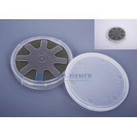
4H Semi-Insulating SiC Substrate With Si Face Cmp Polished, Research Grade,4”Size
PAM-XIAMEN provides high quality single crystal SiC (Silicon Carbide)waferfor electronic and optoelectronic industry. SiC wafer is a next generation semiconductor materialwith unique electrical properties and excellent thermal properties for high temperature and high power device application. SiC wafer can be supplied in diameter 2~6 inch, both 4H and 6H SiC , N-type , Nitrogen doped , and semi-insulating type available.
Please contact us for more information:
SILICON CARBIDE MATERIAL PROPERTIES
| Polytype | Single Crystal 4H | Single Crystal 6H |
| Lattice Parameters | a=3.076 Å | a=3.073 Å |
| c=10.053 Å | c=15.117 Å | |
| Stacking Sequence | ABCB | ABCACB |
| Band-gap | 3.26 eV | 3.03 eV |
| Density | 3.21 · 103 kg/m3 | 3.21 · 103 kg/m3 |
| Therm. Expansion Coefficient | 4-5×10⁻⁶/K | 4-5×10⁻⁶/K |
| Refraction Index | no = 2.719 | no = 2.707 |
| ne = 2.777 | ne = 2.755 | |
| Dielectric Constant | 9.6 | 9.66 |
| Thermal Conductivity | 490 W/mK | 490 W/mK |
| Break-Down Electrical Field | 2-4 · 108 V/m | 2-4 · 108 V/m |
| Saturation Drift Velocity | 2.0 · 105 m/s | 2.0 · 105 m/s |
| Electron Mobility | 800 cm2/V·S | 400 cm2/V·S |
| hole Mobility | 115 cm2/V·S | 90 cm2/V·S |
| Mohs Hardness | ~9 | ~9 |
4H Semi-Insulating SIC Substrate, Research Grade,4”Size
| SUBSTRATE PROPERTY | S4H-51-SI-PWAM-250 S4H-51-SI-PWAM-330 S4H-51-SI-PWAM-430 |
| Description | Research Grade 4H SEMI Substrate |
| Polytype | 4H |
| Diameter | (50.8 ± 0.38) mm |
| Thickness | (250 ± 25) μm (330 ± 25) μm (430 ± 25) μm |
| Resistivity (RT) | >1E5 Ω·cm |
| Surface Roughness | < 0.5 nm (Si-face CMP Epi-ready); <1 nm (C- face Optical polish) |
| FWHM | <50 arcsec |
| Micropipe Density | A+≤1cm-2 A≤10cm-2 B≤30cm-2 C≤50cm-2 D≤100cm-2 |
| Surface Orientation | |
| On axis <0001>± 0.5° | |
| Off axis 3.5° toward <11-20>± 0.5° | |
| Primary flat orientation | Parallel {1-100} ± 5° |
| Primary flat length | 16.00 ± 1.70 mm |
| Secondary flat orientation Si-face:90° cw. from orientation flat ± 5° | |
| C-face:90° ccw. from orientation flat ± 5° | |
| Secondary flat length | 8.00 ± 1.70 mm |
| Surface Finish | Single or double face polished |
| Packaging | Single wafer box or multi wafer box |
| Usable area | ≥ 90 % |
| Edge exclusion | 1 mm |
sic crystal defects
Most of the defects which were observed in SiC were also observed in other crystalline materials. Like the dislocations, stacking faults (SFs), low angle boundaries (LABs) and twins. Some others appear in materials having the Zing- Blend or the Wurtzite structure, like the IDBs. Micropipes and inclusions from other phases mainly appear in SiC.
Choice of Polytype for Devices
As discussed in Section 4, 4H- and 6H-SiC are the far superior forms of semiconductor device quality SiC commercially available in mass-produced wafer form. Therefore, only 4H- and 6H-SiC device processing methods will be explicitly considered in the rest of this section. It should be noted, however, that most of the processing methods discussed in this section are applicable to other polytypes of SiC, except for the case of a 3C-SiC layer still residing on a silicon substrate, where all processing temperatures need to be kept well below the melting temperature of silicon (~1400°C). It is generally accepted that 4H-SiC’s substantially higher carrier mobility and shallower dopant ionization energies compared to 6H-SiC (Table 5.1) should make it the polytype of choice for most SiC electronic devices, provided that all other device processing,performance, and cost-related issues play out as being roughly equal between the two polytypes. Furthermore, the inherent mobility anisotropy that degrades conduction parallel to the crystallographic c-axis in 6H-SiC particularly favors 4H-SiC for vertical power device configurations (Section the 5.6.4). Because the ionization energy of the p-type acceptor dopants is significantly deeper than for the n-type donors, a much higher conductivity can be obtained for the n-type SiC substrates than for the p-type substrates.


